- 您现在的位置:买卖IC网 > PDF目录11153 > MAX4636EUB+T (Maxim Integrated Products)IC SWITCH DUAL SPDT 10UMAX PDF资料下载
参数资料
| 型号: | MAX4636EUB+T |
| 厂商: | Maxim Integrated Products |
| 文件页数: | 4/11页 |
| 文件大小: | 0K |
| 描述: | IC SWITCH DUAL SPDT 10UMAX |
| 产品培训模块: | Lead (SnPb) Finish for COTS Obsolescence Mitigation Program |
| 标准包装: | 2,500 |
| 功能: | 开关 |
| 电路: | 2 x SPDT |
| 导通状态电阻: | 4 欧姆 |
| 电压电源: | 单电源 |
| 电压 - 电源,单路/双路(±): | 1.8 V ~ 5.5 V |
| 电流 - 电源: | 1µA |
| 工作温度: | -40°C ~ 85°C |
| 安装类型: | 表面贴装 |
| 封装/外壳: | 10-TFSOP,10-MSOP(0.118",3.00mm 宽) |
| 供应商设备封装: | 10-µMAX |
| 包装: | 带卷 (TR) |
MAX4635/MAX4636
Fast, Low-Voltage, Dual 4
SPDT
CMOS Analog Switches
2
_______________________________________________________________________________________
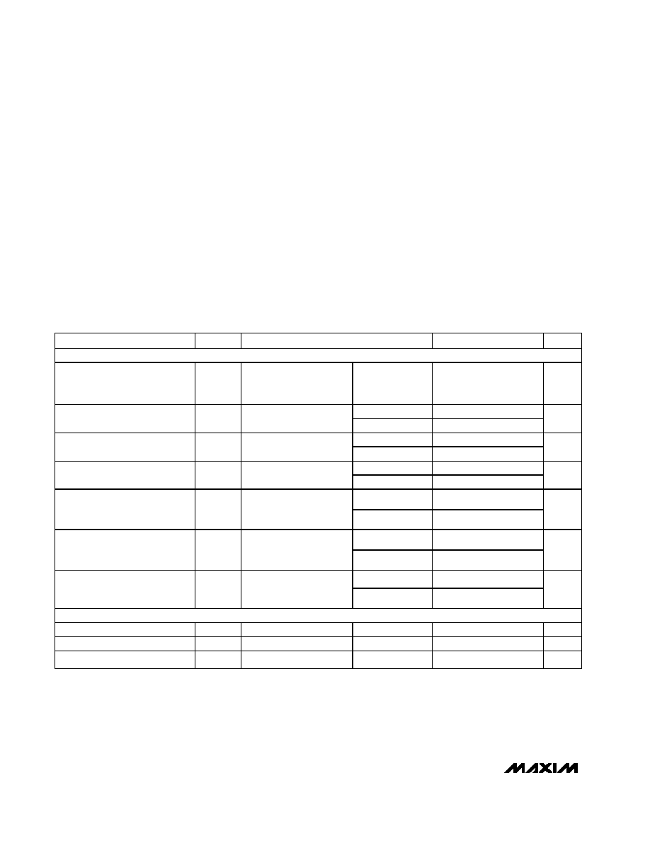
ABSOLUTE MAXIMUM RATINGS
ELECTRICAL CHARACTERISTICS—Single +5V Supply
(V+ = +4.5V to +5.5V, VIH = +2.4V, VIL = +0.8V, TA = TMIN to TMAX, unless otherwise noted. Typical values are at TA = +25°C.)
(Notes 2, 9)
Stresses beyond those listed under “Absolute Maximum Ratings” may cause permanent damage to the device. These are stress ratings only, and functional
operation of the device at these or any other conditions beyond those indicated in the operational sections of the specifications is not implied. Exposure to
absolute maximum rating conditions for extended periods may affect device reliability.
(Voltages Referenced to GND)
V+, IN_ .....................................................................-0.3V to +6V
COM_, NC_, NO_ (Note 1) .......................... -0.3V to (V+ + 0.3V)
Continuous Current into Any Terminal .............................±30mA
Peak Current into COM_, NC_, NO_
(pulsed at 1ms, 10% duty cycle).................................±100mA
Continuous Power Dissipation (TA = +70°C)
10-Pin MAX (derate 4.7mW/°C above +70°C) ............330mW
10-Pin Thin QFN (derate 24.4mW/°C above +70°C) ..1951mW
Operating Temperature Range .......................... -40°C to +85°C
Storage Temperature Range ........................... -65°C to +150°C
Lead Temperature (soldering, 10s) ............................... +300°C
Note 1: Signals on NO_, NC_, or COM_ exceeding V+ or GND are clamped by internal diodes. Limit forward-diode current to maxi-
mum current rating.
PARAMETER
SYMBOL
CONDITIONS
MIN
TYP
MAX
UNITS
ANALOG SWITCH
Analog Signal Range
VCOM_,
VNO_,
VNC_
0V+
V
TA = +25°C
2.5
4
On-Resistance
RON
V+ = 4.5V, ICOM_ = 10mA,
VNO_ or VNC_ = 0 to V+
TA = TMIN to TMAX
4.5
TA = +25°C
0.1
0.2
On-Resistance Match
Between Channels (Notes 3, 4)
RON
V+ = 4.5V, ICOM_ = 10mA,
VNO_ or VNC_ = 0 to V+
TA = TMIN to TMAX
0.4
TA = +25°C
0.5
1
On-Resistance Flatness
(Note 5)
RFLAT(ON)
V+ = 4.5V, ICOM_ = 10mA,
VNO_ or VNC_ = 0 to V+
TA = TMIN to TMAX
1.2
TA = +25°C-0.1
±0.01
0.1
NO_, NC_ Off-Leakage Current
(Note 6)
INC_(OFF),
INO_(OFF)
V+ = 5.5V; VCOM_ = 1V,
4.5V; VNO_ or VNC_ = 4.5V,
1V
TA = TMIN to TMAX
-0.3
0.3
nA
TA = +25°C-0.1
±0.01
0.1
COM_ Off-Leakage Current
(Note 6)
ICOM_(OFF)
V+ = 5.5V; VCOM_ = 1V,
4.5V; VNO_ or VNC_ = 4.5V,
1V
TA = TMIN to TMAX
-0.3
0.3
nA
TA = +25°C-0.1
±0.01
0.1
COM_ On-Leakage Current
(Note 6)
ICOM_(ON)
V+ = 5.5V; VCOM_ = 4.5V,
1V; VNO_ or VNC_ = 4.5V,
1V or floating
TA = TMIN to TMAX
-0.3
0.3
nA
DIGITAL I/O (IN1, IN2)
Input Logic High
VIH
2.4
V
Input Logic Low
VIL
0.8
V
Input Leakage Current
IIH, IIL
VIN_ = 0 or +5.5V
-100
5
100
nA
相关PDF资料 |
PDF描述 |
|---|---|
| VI-B6K-IW-F2 | CONVERTER MOD DC/DC 40V 100W |
| MAX4635EUB+T | IC SWITCH DUAL SPDT 10UMAX |
| VI-B6J-IX-F4 | CONVERTER MOD DC/DC 36V 75W |
| VI-B6J-IX-F1 | CONVERTER MOD DC/DC 36V 75W |
| VI-B11-IY-F4 | CONVERTER MOD DC/DC 12V 50W |
相关代理商/技术参数 |
参数描述 |
|---|---|
| MAX4636EUB-TG069 | 制造商:Rochester Electronics LLC 功能描述: 制造商:Maxim Integrated Products 功能描述: |
| MAX4636EUB-TG075 | 制造商:Rochester Electronics LLC 功能描述: 制造商:Maxim Integrated Products 功能描述: |
| MAX4638EGE | 制造商:Rochester Electronics LLC 功能描述: 制造商:Maxim Integrated Products 功能描述: |
| MAX4638EGP | 制造商:Rochester Electronics LLC 功能描述: 制造商:Maxim Integrated Products 功能描述: |
| MAX4638ESE | 功能描述:多路器开关 IC RoHS:否 制造商:Texas Instruments 通道数量:1 开关数量:4 开启电阻(最大值):7 Ohms 开启时间(最大值): 关闭时间(最大值): 传播延迟时间:0.25 ns 工作电源电压:2.3 V to 3.6 V 工作电源电流: 最大工作温度:+ 85 C 安装风格:SMD/SMT 封装 / 箱体:UQFN-16 |
发布紧急采购,3分钟左右您将得到回复。