- 您现在的位置:买卖IC网 > PDF目录11389 > MAX4656EUA+ (Maxim Integrated Products)IC SWITCH SPST 8UMAX PDF资料下载
参数资料
| 型号: | MAX4656EUA+ |
| 厂商: | Maxim Integrated Products |
| 文件页数: | 5/12页 |
| 文件大小: | 0K |
| 描述: | IC SWITCH SPST 8UMAX |
| 产品培训模块: | Lead (SnPb) Finish for COTS Obsolescence Mitigation Program |
| 标准包装: | 50 |
| 功能: | 开关 |
| 电路: | 1 x SPST- NO |
| 导通状态电阻: | 10 欧姆 |
| 电压电源: | 单/双电源 |
| 电压 - 电源,单路/双路(±): | 9 V ~ 40 V,±4.5 V ~ 20 V |
| 工作温度: | -40°C ~ 85°C |
| 安装类型: | 表面贴装 |
| 封装/外壳: | 8-TSSOP,8-MSOP(0.118",3.00mm 宽) |
| 供应商设备封装: | 8-uMAX |
| 包装: | 管件 |
MAX4655–MAX4658
High-Current, 10
Ω, SPST, CMOS
Analog Switches
2
_______________________________________________________________________________________
ABSOLUTE MAXIMUM RATINGS
ELECTRICAL CHARACTERISTICS—Dual Supplies
(V+ = +15V, V- = -15V, VIH = 2.4V, VIL = 0.8V, TA = TMIN to TMAX, unless otherwise noted. Typical values are at TA = +25°C.)
(Notes 2, 7, 8)
Stresses beyond those listed under “Absolute Maximum Ratings” may cause permanent damage to the device. These are stress ratings only, and functional
operation of the device at these or any other conditions beyond those indicated in the operational sections of the specifications is not implied. Exposure to
absolute maximum rating conditions for extended periods may affect device reliability.
V+ to GND ..............................................................-0.3V to +44V
V- to GND ...............................................................-44V to +0.3V
V+ to V-...................................................................-0.3V to +44V
All Other Pins to GND (Note 1)..................V- - 0.3V to V+ + 0.3V
Continuous Current, COM, NO, NC
(MAX4655/MAX4656) ..................................................±300mA
Continuous Current, COM, NO, NC
(MAX4657/MAX4658) ..................................................±150mA
Continuous Current, IN .....................................................±30mA
Peak Current, COM, NO, NC
(pulsed at 1ms, 10% duty cycle)
MAX4655/MAX4656.................................................±400mA
(pulsed at 1ms, 10% duty cycle)
MAX4657/MAX4658.................................................±300mA
Continuous Power Dissipation (TA = +70°C)
8-Pin TDFN (derate 24.4mW/°C above +70°C) ........1951mW
8-Pin MAX-EP (derate 10.3mW/°C above +70°C)
MAX4655/MAX4656 .................................................825mW
8-Pin MAX (derate 4.50mW/°C above +70°C)
MAX4657/MAX4658 .................................................362mW
8-Pin SO-EP (derate 18.9mW/°C above +70°C)
MAX4655/MAX4656 ...............................................1509mW
8-Pin SO (derate 5.88mW/°C above +70°C)
MAX4657/MAX4658 .................................................471mW
Operating Temperature Ranges
MAX4655–MAX4658 .......................................-40°C to +85°C
Junction Temperature ......................................................+150°C
Storage Temperature Range .............................-65°C to +150°C
Lead Temperature (soldering, 10s) .................................+300°C
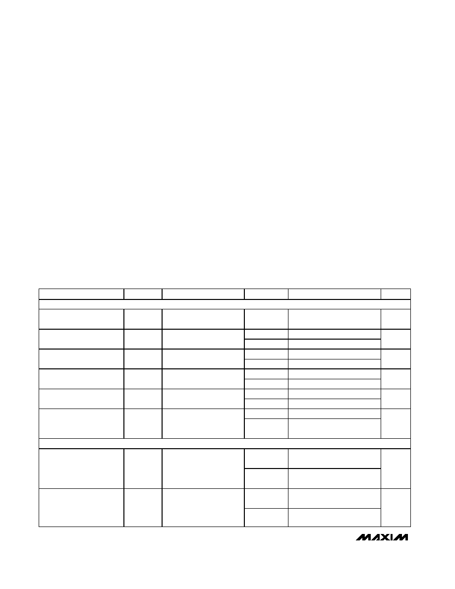
PARAMETER
SYMBOL
CONDITIONS
TA
MIN
TYP
MAX
UNITS
ANALOG SWITCH
Analog Signal Range
VNO, VNC,
VCOM
V-
V+
V
+25°C
7
10
On-Resistance
RON
ICOM = 100mA;
VNO or VNC =
±10V
TMIN to TMAX
15
Ω
+25°C
0.3
1
On-Resistance Flatness
(Note 3)
RFLAT (ON)
ICOM = 100mA;
VNO or VNC = -5V, 0, +5V
TMIN to TMAX
1.5
Ω
+25°C
-1
0.01
+1
NO or NC Off-Leakage
Current (Note 4)
INO(OFF) or
INC(OFF)
VCOM = +14.5V, -14.5V;
VNO or VNC = -14.5V, +14.5V
TMIN to TMAX
-10
10
nA
+25°C
-1
0.01
+1
COM Off-Leakage
Current (Note 4)
ICOM(OFF)
VCOM = +14.5V, -14.5V;
VNO or VNC = -14.5V, +14.5V
TMIN to TMAX
-10
+10
nA
+25°C
-2
+2
COM On-Leakage
Current (Note 4)
ICOM(ON)
VCOM = +14.5V, -14.5V;
VNO or VNC = +14.5V,
-14.5V, or floating
TMIN to TMAX
-20
+20
nA
DYNAMIC CHARACTERISTICS
+25°C
110
200
Turn-On Time
tON
VNO or VNC = 10V;
RL = 50
Ω; MAX4655/4656,
RL = 100
Ω; MAX4657/4658,
CL = 35pF; Figure 3
TMIN to TMAX
300
ns
+25°C
75
100
Turn-Off Time
tOFF
VNO or VNC = 10V;
RL = 50
Ω; MAX4655/4656,
RL = 100
Ω; MAX4657/4658,
CL = 35pF; Figure 3
TMIN to TMAX
150
ns
Note 1: Signals on NC, NO, COM, or IN exceeding V+ or V- will be clamped by internal diodes. Limit forward diode current to max-
imum current rating.
相关PDF资料 |
PDF描述 |
|---|---|
| DG419DY+ | IC SWITCH SPDT 8SOIC |
| DEA1X3A270JP2A | CAP CER 27PF 1KV 5% RADIAL |
| MAX4052AESE+ | IC MULTIPLEXER DUAL 4X1 16SOIC |
| DEA1X3A220JP2A | CAP CER 22PF 1KV 5% RADIAL |
| VI-26Z-IY | CONVERTER MOD DC/DC 2V 20W |
相关代理商/技术参数 |
参数描述 |
|---|---|
| MAX4656EUA+ | 功能描述:模拟开关 IC 10Ohm SPST CMOS Analog Switch RoHS:否 制造商:Texas Instruments 开关数量:2 开关配置:SPDT 开启电阻(最大值):0.1 Ohms 切换电压(最大): 开启时间(最大值): 关闭时间(最大值): 工作电源电压:2.7 V to 4.5 V 最大工作温度:+ 85 C 安装风格:SMD/SMT 封装 / 箱体:DSBGA-16 |
| MAX4656EUA+T | 功能描述:模拟开关 IC 10Ohm SPST CMOS Analog Switch RoHS:否 制造商:Texas Instruments 开关数量:2 开关配置:SPDT 开启电阻(最大值):0.1 Ohms 切换电压(最大): 开启时间(最大值): 关闭时间(最大值): 工作电源电压:2.7 V to 4.5 V 最大工作温度:+ 85 C 安装风格:SMD/SMT 封装 / 箱体:DSBGA-16 |
| MAX4656EUA-T | 功能描述:模拟开关 IC RoHS:否 制造商:Texas Instruments 开关数量:2 开关配置:SPDT 开启电阻(最大值):0.1 Ohms 切换电压(最大): 开启时间(最大值): 关闭时间(最大值): 工作电源电压:2.7 V to 4.5 V 最大工作温度:+ 85 C 安装风格:SMD/SMT 封装 / 箱体:DSBGA-16 |
| MAX4657ESA | 功能描述:模拟开关 IC RoHS:否 制造商:Texas Instruments 开关数量:2 开关配置:SPDT 开启电阻(最大值):0.1 Ohms 切换电压(最大): 开启时间(最大值): 关闭时间(最大值): 工作电源电压:2.7 V to 4.5 V 最大工作温度:+ 85 C 安装风格:SMD/SMT 封装 / 箱体:DSBGA-16 |
| MAX4657ESA+ | 功能描述:模拟开关 IC 10Ohm SPST CMOS Analog Switch RoHS:否 制造商:Texas Instruments 开关数量:2 开关配置:SPDT 开启电阻(最大值):0.1 Ohms 切换电压(最大): 开启时间(最大值): 关闭时间(最大值): 工作电源电压:2.7 V to 4.5 V 最大工作温度:+ 85 C 安装风格:SMD/SMT 封装 / 箱体:DSBGA-16 |
发布紧急采购,3分钟左右您将得到回复。