- 您现在的位置:买卖IC网 > PDF目录4592 > MAX4670ETJ+ (Maxim Integrated Products)IC PROT SWITCH T1/E1/J1 32-TQFN PDF资料下载
参数资料
| 型号: | MAX4670ETJ+ |
| 厂商: | Maxim Integrated Products |
| 文件页数: | 12/20页 |
| 文件大小: | 0K |
| 描述: | IC PROT SWITCH T1/E1/J1 32-TQFN |
| 产品培训模块: | Lead (SnPb) Finish for COTS Obsolescence Mitigation Program Low Voltage Analog Switches Overview |
| 标准包装: | 60 |
| 系列: | * |
| 类型: | * |
| 应用: | * |
| 安装类型: | 表面贴装 |
| 封装/外壳: | 32-WFQFN 裸露焊盘 |
| 供应商设备封装: | 32-TQFN-EP(5x5) |
| 包装: | 管件 |
MAX4670
Integrated T1/E1/J1 Short-Haul and
Long-Haul Protection Switch
2
_______________________________________________________________________________________
ABSOLUTE MAXIMUM RATINGS
Stresses beyond those listed under “Absolute Maximum Ratings” may cause permanent damage to the device. These are stress ratings only, and functional
operation of the device at these or any other conditions beyond those indicated in the operational sections of the specifications is not implied. Exposure to
absolute maximum rating conditions for extended periods may affect device reliability.
(All voltages referenced to GND.)
V+, IN_, SWITCH ......................................................-0.3V to +4V
COM_, NO_, NC_ (Note 1) ...........................-0.3V to (V+ + 0.3V)
Continuous Current
NO_, NC_, COM_ (Tx interface)..................................
±150mA
NO_, NC_, COM_ (Rx interface) .................................
±100mA
Peak Currents
NO_, NC_, COM_ (Tx interface)
(pulsed at 1ms, 10% duty cycle) ................................
±300mA
NO_, NC_, COM_ (Rx interface)
(pulsed at 1ms, 10% duty cycle) ................................
±200mA
Peak Surge Currents
Poised at 8s ..................................................................21.4A
Poised at 20s ................................................................11.9A
Continuous Power Dissipation (TA = +70°C)
32-Pin TQFN (derate 21.3mW/°C above +70°C) .......1702mW
38-Pin TSSOP (derate 13.7mW/°C above +70°C) .....1096mW
Operating Temperature Range ...........................-40°C to +85°C
Storage Temperature Range .............................-65°C to +150°C
Junction Temperature ......................................................+150°C
Lead Temperature (soldering, 10s) .................................+300°C
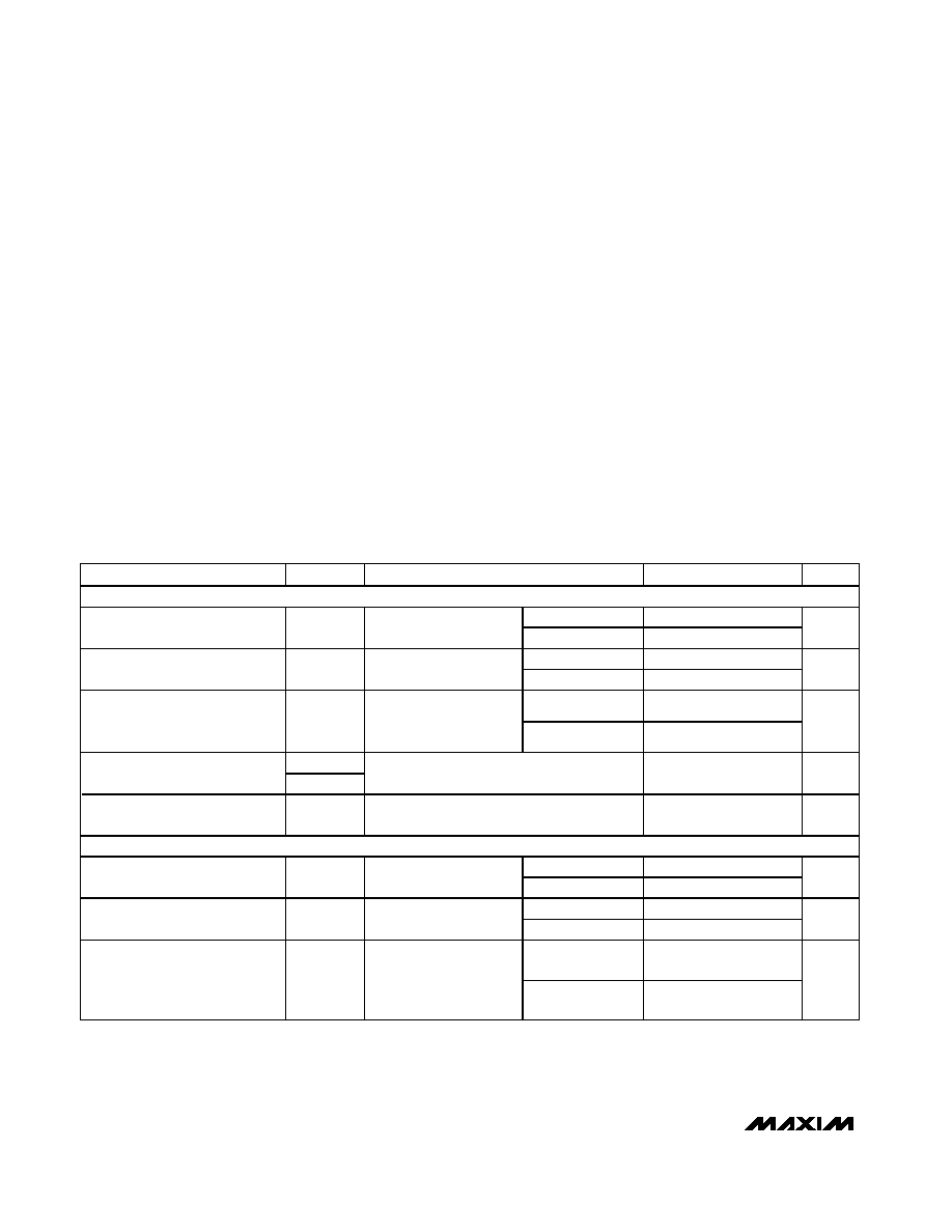
ELECTRICAL CHARACTERISTICS
(V+ = +2.7V to +3.6V, TA = TMIN to TMAX, unless otherwise noted. Typical values are at TA = +25°C, unless otherwise noted.) (Notes 2, 3)
PARAMETER
SYMBOL
CONDITIONS
MIN
TYP
MAX
UNITS
Rx INTERFACE
TA = +25°C5
9
On-Resistance
RON
V+ = 3V, ICOM_ = 10mA,
VNO_ or VNC_ = 1.5V
TA = TMIN to TMAX
10
TA = +25°C
1.0
On-Resistance Match Between
Channels (Note 4)
RON
V+ = 3V, ICOM_ = 10mA,
VNO_ or VNC_ = 1.5V
TA = TMIN to TMAX
1.3
TA = +25°C
2.0
3.0
On-Resistance Flatness (Note 4)
RFLAT(ON)
V+ = 3V; ICOM_ = 10mA;
VNO_ or VNC_ = 1.0V,
1.5V, 2.0V
TA = TMIN to TMAX
3.4
INO(OFF)
NO_ or NC_ Off-Leakage
Current
INC (OFF)
V+ = 3.6V; VCOM_ = 0.3V, 3.3V;
VNO_ or VNC_ = 3.3V, 0.3V
-1
+1
A
COM_ On-Leakage Current
ICOM(ON)
V+ = 3.6V; VCOM_ = 0.3V, 3.3V;
VNO_ or VNC_ = 3.3V, 0.3V or floating
-1
+1
A
Tx INTERFACE
TA = +25°C
0.7
0.9
On-Resistance (Note 5)
RON
V+ = 3V, ICOM_ = 100mA,
VNO_ or VNC_ = 1.5V
TA = TMIN to TMAX
1.0
TA = +25°C
0.03
0.150
On-Resistance Match Between
Channels (Notes 3, 5)
RON
V+ = 3V, ICOM_ = 100mA,
VNO_ or VNC_ = 1.5V
TA = TMIN to TMAX
0.175
TA = +25°C
0.1
0.18
On-Resistance Flatness
(Notes 5, 6)
RFLAT(ON)
V+ = 3V;
ICOM_ = 100mA;
VNO_ or VNC_ = 1.0V,
1.5V, 2.0V
TA = TMIN to TMAX
0.2
Note 1: Signals on NO_, NC_, COM_ exceeding V+ or GND are clamped by internal diodes. Limit forward-diode current to maximum
current rating.
相关PDF资料 |
PDF描述 |
|---|---|
| MAX4507CAP+ | IC SIGNAL LINE PROTECTOR 20-SSOP |
| LFEC6E-4TN144I | IC FPGA 6.1KLUTS 97I/O 144-TQFP |
| MAX4507CPN+ | IC SIGNAL LINE PROTECTOR 18-DIP |
| DS1402-BR8+ | CABLE 8' BUTTON TO RJ11 |
| LFXP6E-3F256C | IC FPGA 5.8KLUTS 188I/O 256-BGA |
相关代理商/技术参数 |
参数描述 |
|---|---|
| MAX4670ETJ+ | 功能描述:模拟开关 IC Integrated T1/E1/J1 rotection Switch RoHS:否 制造商:Texas Instruments 开关数量:2 开关配置:SPDT 开启电阻(最大值):0.1 Ohms 切换电压(最大): 开启时间(最大值): 关闭时间(最大值): 工作电源电压:2.7 V to 4.5 V 最大工作温度:+ 85 C 安装风格:SMD/SMT 封装 / 箱体:DSBGA-16 |
| MAX4670ETJ+T | 功能描述:模拟开关 IC Integrated T1/E1/J1 rotection Switch RoHS:否 制造商:Texas Instruments 开关数量:2 开关配置:SPDT 开启电阻(最大值):0.1 Ohms 切换电压(最大): 开启时间(最大值): 关闭时间(最大值): 工作电源电压:2.7 V to 4.5 V 最大工作温度:+ 85 C 安装风格:SMD/SMT 封装 / 箱体:DSBGA-16 |
| MAX4670ETJ-T | 功能描述:模拟开关 IC RoHS:否 制造商:Texas Instruments 开关数量:2 开关配置:SPDT 开启电阻(最大值):0.1 Ohms 切换电压(最大): 开启时间(最大值): 关闭时间(最大值): 工作电源电压:2.7 V to 4.5 V 最大工作温度:+ 85 C 安装风格:SMD/SMT 封装 / 箱体:DSBGA-16 |
| MAX4670EUU | 制造商:Maxim Integrated Products 功能描述:- Rail/Tube |
| MAX4670EUU-T | 制造商:Maxim Integrated Products 功能描述:- Tape and Reel |
发布紧急采购,3分钟左右您将得到回复。