- 您现在的位置:买卖IC网 > PDF目录1942 > MAX4674EUE+T (Maxim Integrated Products)IC MULTIPLEXER QUAD 2X1 16TSSOP PDF资料下载
参数资料
| 型号: | MAX4674EUE+T |
| 厂商: | Maxim Integrated Products |
| 文件页数: | 6/13页 |
| 文件大小: | 0K |
| 描述: | IC MULTIPLEXER QUAD 2X1 16TSSOP |
| 产品培训模块: | Lead (SnPb) Finish for COTS Obsolescence Mitigation Program |
| 标准包装: | 2,500 |
| 功能: | 多路复用器 |
| 电路: | 4 x 2:1 |
| 导通状态电阻: | 4 欧姆 |
| 电压电源: | 单电源 |
| 电压 - 电源,单路/双路(±): | 1.8 V ~ 5.5 V |
| 电流 - 电源: | 1µA |
| 工作温度: | -40°C ~ 85°C |
| 安装类型: | 表面贴装 |
| 封装/外壳: | 16-TSSOP(0.173",4.40mm 宽) |
| 供应商设备封装: | 16-TSSOP |
| 包装: | 带卷 (TR) |
MAX4674
3V/5V, 4
, Wideband Quad
2:1 Analog Multiplexer
2
_______________________________________________________________________________________
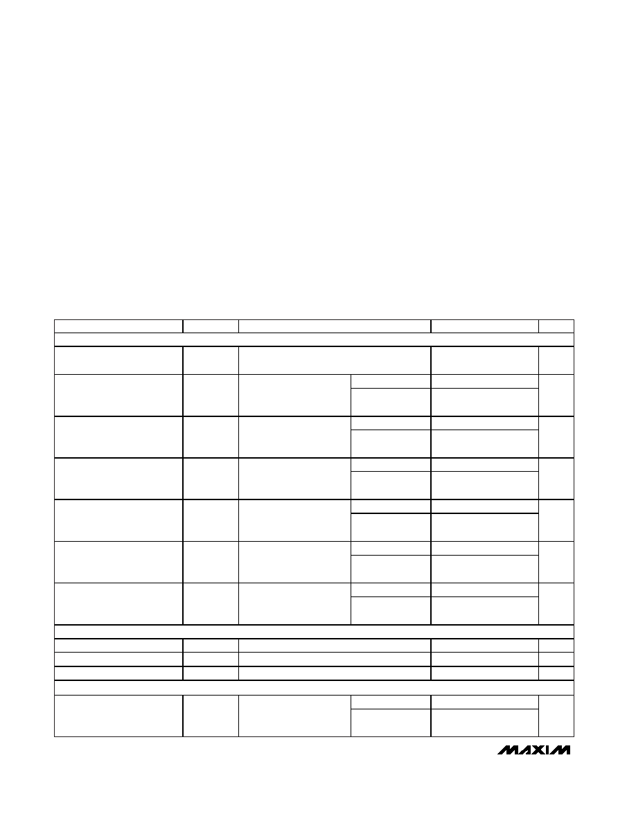
ABSOLUTE MAXIMUM RATINGS
ELECTRICAL CHARACTERISTICS—Single +5V Supply
(V+ = +4.5V to +5.5V, VIH = 2.4V, VIL = 0.8V, TA = TMIN to TMAX, unless otherwise noted. Typical values at TA = +25°C.) (Notes 2, 3)
Stresses beyond those listed under “Absolute Maximum Ratings” may cause permanent damage to the device. These are stress ratings only, and functional
operation of the device at these or any other conditions beyond those indicated in the operational sections of the specifications is not implied. Exposure to
absolute maximum rating conditions for extended periods may affect device reliability.
V+, A0, EN................................................................-0.3V to +6V
COM_, NO_, NC_ (Note1)...............................-0.3V to (V + 0.3V)
Continuous Current COM_, NO_, NC_ ..........................±100mA
Peak Current (COM_, NO_, NC_)
(pulsed at 1ms, 10% duty cycle) ..............................±300mA
Continuous Power Dissipation (TA = +70°C)
16-Pin QSOP (derate 8.3mW/°C above +70°C) ........ 667mW
16-Pin TSSOP (derate 6.7mW/°C above +70°C) .......533mW
16-Pin Narrow SO (derate 8mW/°C above +70°C) ....640mW
16-Pin QFN (derate 18.5mW/°C above +70°C) ........1481mW
20-Pin QFN (derate 20mW/°C above +70°C) ...........1600mW
Operating Temperature Range
MAX4674E_E .................................................-40°C to +85°C
Die Temperature ..............................................................+150°C
Storage Temperature Range ............................-65°C to +150°C
Lead Temperature (soldering, 10s) ................................+300°C
Note 1: Signals on NO_, NC_, and COM_ exceeding V+ or GND are clamped by internal diodes. Limit forward-diode current to max-
imum current rating.
PARAMETER
SYMBOL
CONDITIONS
MIN
TYP
MAX
UNITS
ANALOG SWITCH
Analog Signal Range
VCOM_,VNO_,
VNC_
0V+
V
TA = +25°C
2.2
4
On-Resistance
RON
V+ = 4.5V, ICOM_ = 10mA,
VNO_ or VNC_ = 0 to V+
TA = TMIN to
TMAX
5
TA = +25°C
0.15
0.4
On-Resistance Match Between
Channels (Notes 4, 5)
RON
V+ = 4.5V, ICOM_ = 10mA,
VNO_ or VNC_ = 0 to V+
TA = TMIN to
TMAX
0.5
TA = +25°C
0.5
0.8
On-Resistance Flatness
(Note 6)
RFLAT (ON)
V+ = 4.5V, ICOM_ = 10mA,
VNO_ or VNC_ = 0 to V+
TA = TMIN to
TMAX
1
TA = +25°C
-0.5
±0.01
+0.5
NO_, NC_ Off-Leakage
Current (Note 7)
INO_(OFF),
INC_(OFF)
V+ = 5.5V; VCOM_ = 1V,
4.5V; VNO_ or VNC_ = 4.5V,
1V
TA = TMIN to
TMAX
-1
+1
nA
TA = +25°C
-0.5
±0.01
+0.5
COM_ Off-Leakage Current
(Note 7)
ICOM_(OFF)
V+ = 5.5V; VCOM_ = 1V,
4.5V; VNO_ or VNC_ = 4.5V,
1V
TA = TMIN to
TMAX
-1
+1
nA
TA = +25°C
-0.5
±0.01
+0.5
COM_ On-Leakage Current
(Note 7)
ICOM_(ON)
V+ = 5.5V; VCOM_ = 1V,
4.5V; VNO_ or VNC_ = 1,
4.5V, or floating
TA = TMIN to
TMAX
-1
+1
nA
DIGITAL I/O (A0, EN)
Input Logic High
VIH
2.4
V
Input Logic Low
VIL
0.8
V
Input Leakage Current
IIN
VIN = 0 or +5.5V
-0.5
±1
+0.5
A
DYNAMIC
TA = +25°C
10
18
Turn-On Time (Note 7)
tON
VNO_ or VNC_ = 3V,
RL = 100
, CL = 35pF,
Figure 2
TA = TMIN to
TMAX
20
ns
相关PDF资料 |
PDF描述 |
|---|---|
| MAX4675EUT+T | IC ANALOG SWITCH SPST SOT23-6 |
| MAX4679EUE+T | IC SWITCH QUAD SPST 16TSSOP |
| MAX4685EUB | IC SWITCH DUAL SPDT 10UMAX |
| MAX4688EBT+T | IC SWITCH SPDT 6UCSP |
| MAX4691EGE-T | IC MULTIPLEXER 8X1 16QFN |
相关代理商/技术参数 |
参数描述 |
|---|---|
| MAX4675EUT | 制造商:Maxim Integrated Products 功能描述:6 PIN COUNT SOT PACKAGE TYPE - Rail/Tube |
| MAX4675EUT+ | 制造商:Maxim Integrated Products 功能描述: 制造商:Maxim Integrated Products 功能描述:ANLG SW SGL SPST 5.5V/5.5V 6PIN SOT-23 - Cut Tape Product |
| MAX4675EUT+T | 功能描述:模拟开关 IC 3Ohm Single SPST Analog Switch RoHS:否 制造商:Texas Instruments 开关数量:2 开关配置:SPDT 开启电阻(最大值):0.1 Ohms 切换电压(最大): 开启时间(最大值): 关闭时间(最大值): 工作电源电压:2.7 V to 4.5 V 最大工作温度:+ 85 C 安装风格:SMD/SMT 封装 / 箱体:DSBGA-16 |
| MAX4675EUT-T | 功能描述:模拟开关 IC RoHS:否 制造商:Texas Instruments 开关数量:2 开关配置:SPDT 开启电阻(最大值):0.1 Ohms 切换电压(最大): 开启时间(最大值): 关闭时间(最大值): 工作电源电压:2.7 V to 4.5 V 最大工作温度:+ 85 C 安装风格:SMD/SMT 封装 / 箱体:DSBGA-16 |
| MAX4676EUT | 制造商:Maxim Integrated Products 功能描述:- Cut Tape Product |
发布紧急采购,3分钟左右您将得到回复。