- 您现在的位置:买卖IC网 > PDF目录11131 > MAX4677EUE+T (Maxim Integrated Products)IC SWITCH QUAD SPST 16TSSOP PDF资料下载
参数资料
| 型号: | MAX4677EUE+T |
| 厂商: | Maxim Integrated Products |
| 文件页数: | 11/12页 |
| 文件大小: | 0K |
| 描述: | IC SWITCH QUAD SPST 16TSSOP |
| 产品培训模块: | Lead (SnPb) Finish for COTS Obsolescence Mitigation Program |
| 标准包装: | 2,500 |
| 功能: | 开关 |
| 电路: | 4 x SPST - NC |
| 导通状态电阻: | 1.6 欧姆 |
| 电压电源: | 单/双电源 |
| 电压 - 电源,单路/双路(±): | 2.7 V ~ 11 V,±2.7 V ~ 5.5 V |
| 工作温度: | -40°C ~ 85°C |
| 安装类型: | 表面贴装 |
| 封装/外壳: | 16-TSSOP(0.173",4.40mm 宽) |
| 供应商设备封装: | 16-TSSOP |
| 包装: | 带卷 (TR) |
MAX4677/MAX4678/MAX4679
2
, Quad, SPST, CMOS Analog Switches
8
_______________________________________________________________________________________
___________Applications Information
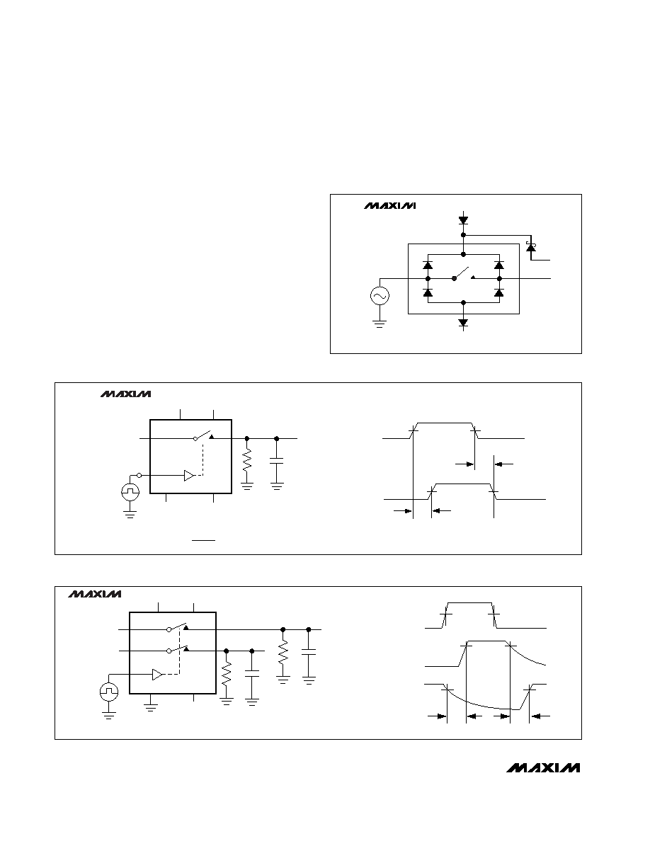
Overvoltage Protection
Proper power-supply sequencing is recommended for
all CMOS devices. Do not exceed the absolute maxi-
mum ratings because stresses beyond the listed ratings
can cause permanent damage to the devices. Always
sequence V+ on first, then V-, then VL followed by the
logic inputs, NO_, NC_, or COM. If proper power-supply
sequencing is not possible, add two small signal diodes
(D1, D2) in series with the supply pins, and a Schottky
diode between V+ and VL for overvoltage protection
(Figure 1). Adding diodes reduces the analog signal
range to one diode drop below V+ and one diode drop
above V-, but does not affect the devices’ low switch
resistance and low leakage characteristics. Device oper-
ation is unchanged, and the difference between V+ and
V- should not exceed 11V.
Power-supply bypassing improves noise margin and
prevents switching noise from propagating from the V+
supply to other components. A 0.1F capacitor connect-
ed from V+ to GND is adequate for most applications.
Figure 1. Overvoltage Protection Using External Blocking Diodes
COM_
V2
V-
V+
NO_
VL
D1
D2
*
*INTERNAL PROTECTION DIODES
MAX4677
MAX4678
MAX4679
tr < 20ns
tf < 20ns
50%
0
LOGIC
INPUT
V-
RL
300
NO_
OR NC_
GND
CL INCLUDES FIXTURE AND STRAY CAPACITANCE.
VOUT = VCOM
(
RL
)
RL + RON
SWITCH
INPUT
IN_
+3V
tOFF
0
COM_
SWITCH
OUTPUT
0.9 x V0UT
0.9 x VOUT
tON
VOUT
SWITCH
OUTPUT
LOGIC
INPUT
CL
35pF
V+
VL
VOUT
VCOM
0V
MAX4677
MAX4678
MAX4679
Figure 2. Switching Time
50%
0.9 x V0UT1
+3V
0
LOGIC
INPUT
SWITCH
OUTPUT 2
(VOUT2)
0
0.9 x VOUT2
tD
LOGIC
INPUT
V-
RL2
GND
CL INCLUDES FIXTURE AND STRAY CAPACITANCE.
COM2
IN1
COM1
VOUT2
V+
CL2
VCOM1 = +3V
RL1
VOUT1
CL1
RL = 300
CL = 35pF
NO1
NC2
SWITCH
OUTPUT 1
(VOUT1)
MAX4679
VCOM2 = +3V
V+
VL
IN2
Figure 3. Break-Before-Make Interval (MAX4679 Only)
相关PDF资料 |
PDF描述 |
|---|---|
| IH5040CWE+T | IC SWITCH SPST 16SOIC |
| MAX4760EBX+T | IC SWITCH QUAD DPDT 36UCSP |
| MAX4593EUE+T | IC SWITCH QUAD SPST 16TSSOP |
| VI-B6R-IX-F2 | CONVERTER MOD DC/DC 7.5V 75W |
| MAX4760EWX+T | IC SWITCH QUAD DPDT 36WLP |
相关代理商/技术参数 |
参数描述 |
|---|---|
| MAX4678EPE | 功能描述:模拟开关 IC RoHS:否 制造商:Texas Instruments 开关数量:2 开关配置:SPDT 开启电阻(最大值):0.1 Ohms 切换电压(最大): 开启时间(最大值): 关闭时间(最大值): 工作电源电压:2.7 V to 4.5 V 最大工作温度:+ 85 C 安装风格:SMD/SMT 封装 / 箱体:DSBGA-16 |
| MAX4678EPE+ | 功能描述:模拟开关 IC 2Ohm Quad SPST CMOS Analog Switch RoHS:否 制造商:Texas Instruments 开关数量:2 开关配置:SPDT 开启电阻(最大值):0.1 Ohms 切换电压(最大): 开启时间(最大值): 关闭时间(最大值): 工作电源电压:2.7 V to 4.5 V 最大工作温度:+ 85 C 安装风格:SMD/SMT 封装 / 箱体:DSBGA-16 |
| MAX4678EUE | 功能描述:模拟开关 IC RoHS:否 制造商:Texas Instruments 开关数量:2 开关配置:SPDT 开启电阻(最大值):0.1 Ohms 切换电压(最大): 开启时间(最大值): 关闭时间(最大值): 工作电源电压:2.7 V to 4.5 V 最大工作温度:+ 85 C 安装风格:SMD/SMT 封装 / 箱体:DSBGA-16 |
| MAX4678EUE+ | 功能描述:模拟开关 IC 2Ohm Quad SPST CMOS Analog Switch RoHS:否 制造商:Texas Instruments 开关数量:2 开关配置:SPDT 开启电阻(最大值):0.1 Ohms 切换电压(最大): 开启时间(最大值): 关闭时间(最大值): 工作电源电压:2.7 V to 4.5 V 最大工作温度:+ 85 C 安装风格:SMD/SMT 封装 / 箱体:DSBGA-16 |
| MAX4678EUE+T | 功能描述:模拟开关 IC 2Ohm Quad SPST CMOS Analog Switch RoHS:否 制造商:Texas Instruments 开关数量:2 开关配置:SPDT 开启电阻(最大值):0.1 Ohms 切换电压(最大): 开启时间(最大值): 关闭时间(最大值): 工作电源电压:2.7 V to 4.5 V 最大工作温度:+ 85 C 安装风格:SMD/SMT 封装 / 箱体:DSBGA-16 |
发布紧急采购,3分钟左右您将得到回复。