- 您现在的位置:买卖IC网 > PDF目录11143 > MAX4701ETE+T (Maxim Integrated Products)IC SWITCH DUAL DPDT 16TQFN PDF资料下载
参数资料
| 型号: | MAX4701ETE+T |
| 厂商: | Maxim Integrated Products |
| 文件页数: | 10/11页 |
| 文件大小: | 0K |
| 描述: | IC SWITCH DUAL DPDT 16TQFN |
| 产品培训模块: | Lead (SnPb) Finish for COTS Obsolescence Mitigation Program |
| 标准包装: | 2,500 |
| 功能: | 开关 |
| 电路: | 2 x DPDT |
| 导通状态电阻: | 75 欧姆 |
| 电压电源: | 单电源 |
| 电压 - 电源,单路/双路(±): | 1.8 V ~ 5.5 V |
| 电流 - 电源: | 1µA |
| 工作温度: | -40°C ~ 85°C |
| 安装类型: | 表面贴装 |
| 封装/外壳: | 16-WFQFN 裸露焊盘 |
| 供应商设备封装: | 16-TQFN-EP(3x3) |
| 包装: | 带卷 (TR) |
MAX4699/MAX4701/MAX4702
Power-Supply Sequencing and
Overvoltage Protection
Caution: Do not exceed the absolute maximum rat-
ings because stresses beyond the listed ratings
may cause permanent damage to the devices.
Proper power-supply sequencing is recommended for
all CMOS devices. Always apply V+ before applying
analog signals, especially if the analog signal is not cur-
rent limited. If this sequencing is not possible, and if the
analog inputs are not current limited to <20mA, add a
small-signal diode (D1) as shown in Figure 1. If the ana-
log signal can dip below GND, add D2. Adding protec-
tion diodes reduces the analog range to a diode drop
(about 0.7V) below V+ (for D1), and a diode drop above
ground (for D2). On-resistance increases slightly at low
supply voltages. Maximum supply voltage (V+) must not
exceed +6V.
Adding protection diode D2 causes the logic threshold
to be shifted relative to GND. TTL compatibility is not
guaranteed when D2 is added.
Protection diodes D1 and D2 also protect against some
overvoltage situations. With Figure 1’s circuit, if the sup-
ply voltage is below the absolute maximum rating, and
if a fault voltage up to the absolute maximum rating is
applied to an analog signal pin, no damage will result.
VL Logic Input (MAX4702)
The MAX4702 features a VL logic input that allows for
lower logic input thresholds down to 1.0V min for VIH in
the quad SPDT configuration. Power-up VL after V+ has
been powered with a minimum of 1.5V to ensure proper
operation of the device.
Low-Voltage, Dual DPDT/Quad SPDT
Analog Switches in QFN
8
_______________________________________________________________________________________
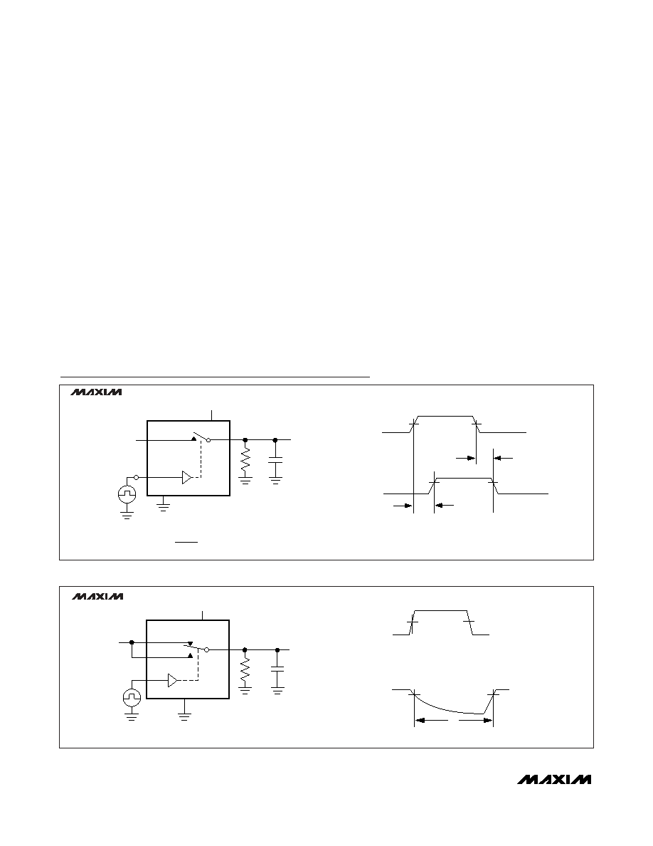
tr < 5ns
tf < 5ns
50%
VIL
LOGIC
INPUT
RL
300
Ω
COM_
GND
IN_
CL INCLUDES FIXTURE AND STRAY CAPACITANCE.
VOUT = VN_
(
RL
)
RL + RON
VN_
VIH
tOFF
0
NO_
OR NC_
0.9 x V0UT
0.9 x VOUT
tON
VOUT
SWITCH
OUTPUT
LOGIC
INPUT
LOGIC INPUT WAVEFORMS INVERTED FOR SWITCHES
THAT HAVE THE OPPOSITE LOGIC SENSE.
V+
CL
35pF
V+
VOUT
MAX4699
MAX4701
MAX4702
Figure 2. Switching Time
50%
VIH
VIL
LOGIC
INPUT
VOUT
0.9 x VOUT
tD
LOGIC
INPUT
RL
300
Ω
GND
CL INCLUDES FIXTURE AND STRAY CAPACITANCE.
NO_
IN_
NC_
VOUT
V+
CL
35pF
VN_
COM_
MAX4699
MAX4701
MAX4702
Figure 3. Break-Before-Make Interval
Test Circuits/Timing Diagrams
相关PDF资料 |
PDF描述 |
|---|---|
| VE-2WZ-IW-F1 | CONVERTER MOD DC/DC 2V 40W |
| MAX4699ETE+T | IC SWITCH DUAL DPDT 16TQFN |
| DG419LDJ+ | IC SWITCH SPDT 8DIP |
| VE-B60-IX-F4 | CONVERTER MOD DC/DC 5V 75W |
| VE-B60-IX-F3 | CONVERTER MOD DC/DC 5V 75W |
相关代理商/技术参数 |
参数描述 |
|---|---|
| MAX4701EUE | 功能描述:模拟开关 IC RoHS:否 制造商:Texas Instruments 开关数量:2 开关配置:SPDT 开启电阻(最大值):0.1 Ohms 切换电压(最大): 开启时间(最大值): 关闭时间(最大值): 工作电源电压:2.7 V to 4.5 V 最大工作温度:+ 85 C 安装风格:SMD/SMT 封装 / 箱体:DSBGA-16 |
| MAX4701EUE+ | 功能描述:模拟开关 IC 2Ch DPDT Analog Switch RoHS:否 制造商:Texas Instruments 开关数量:2 开关配置:SPDT 开启电阻(最大值):0.1 Ohms 切换电压(最大): 开启时间(最大值): 关闭时间(最大值): 工作电源电压:2.7 V to 4.5 V 最大工作温度:+ 85 C 安装风格:SMD/SMT 封装 / 箱体:DSBGA-16 |
| MAX4701EUE+T | 功能描述:模拟开关 IC 2Ch DPDT Analog Switch RoHS:否 制造商:Texas Instruments 开关数量:2 开关配置:SPDT 开启电阻(最大值):0.1 Ohms 切换电压(最大): 开启时间(最大值): 关闭时间(最大值): 工作电源电压:2.7 V to 4.5 V 最大工作温度:+ 85 C 安装风格:SMD/SMT 封装 / 箱体:DSBGA-16 |
| MAX4701EUE-T | 功能描述:模拟开关 IC RoHS:否 制造商:Texas Instruments 开关数量:2 开关配置:SPDT 开启电阻(最大值):0.1 Ohms 切换电压(最大): 开启时间(最大值): 关闭时间(最大值): 工作电源电压:2.7 V to 4.5 V 最大工作温度:+ 85 C 安装风格:SMD/SMT 封装 / 箱体:DSBGA-16 |
| MAX4702EGE | 功能描述:模拟开关 IC RoHS:否 制造商:Texas Instruments 开关数量:2 开关配置:SPDT 开启电阻(最大值):0.1 Ohms 切换电压(最大): 开启时间(最大值): 关闭时间(最大值): 工作电源电压:2.7 V to 4.5 V 最大工作温度:+ 85 C 安装风格:SMD/SMT 封装 / 箱体:DSBGA-16 |
发布紧急采购,3分钟左右您将得到回复。