- 您现在的位置:买卖IC网 > PDF目录11321 > MAX4712EUE+ (Maxim Integrated Products)IC SWITCH QUAD SPST 16TSSOP PDF资料下载
参数资料
| 型号: | MAX4712EUE+ |
| 厂商: | Maxim Integrated Products |
| 文件页数: | 2/17页 |
| 文件大小: | 0K |
| 描述: | IC SWITCH QUAD SPST 16TSSOP |
| 产品培训模块: | Lead (SnPb) Finish for COTS Obsolescence Mitigation Program |
| 标准包装: | 96 |
| 功能: | 开关 |
| 电路: | 4 x SPST - NO |
| 导通状态电阻: | 25 欧姆 |
| 电压电源: | 单/双电源 |
| 电压 - 电源,单路/双路(±): | 2.7 V ~ 11 V,±2.7 V ~ 5.5 V |
| 工作温度: | -40°C ~ 85°C |
| 安装类型: | 表面贴装 |
| 封装/外壳: | 16-TSSOP(0.173",4.40mm 宽) |
| 供应商设备封装: | 16-TSSOP |
| 包装: | 管件 |
MAX4711/MAX4712/MAX4713
Detailed Description
The MAX4711/MAX4712/MAX4713 differ considerably
from traditional fault-protection switches, with several
advantages. First, they are constructed with two paral-
lel FET’s allowing very low on-resistance. Second, they
allow signals on the NC_ or NO_ pins that are within or
slightly beyond the supply rails to be passed through
the switch to the COM terminal, allowing rail-to-rail sig-
nal operation. Third, when a signal on NC_ or NO_
exceeds the supply rails by about 150mV (a fault con-
dition) the voltage on COM_ is limited to the same
polarity supply voltage. Operation is identical for both
fault polarities.
During a fault condition, the NO_ or NC_ input
becomes high impedance regardless of the switch
state or load resistance. If the switch is on, the COM_
output current is supplied from V+ or V- by the clamp
FET’s that are connected from COM to each supply.
These FET’s can typically source or sink up to 15mA.
When power is removed, the fault protection is still in
effect. In this case, the NO_ or NC_ terminals are a vir-
tual open circuit. The fault can be up to ±12V.
The COM_ pins are not fault-protected, they act as nor-
mal CMOS switch terminals. If a voltage source is con-
nected to any COM_ pin, it should be limited to the
supply voltages. Exceeding the supply voltage will
cause high currents to flow through the ESD-protected
diodes, possibly damaging the device (see Absolute
Maximum Ratings).
Pin Compatibility
These switches have identical pinouts to common non-
fault-protected CMOS switches. Care should be exer-
cised while considering them for direct replacements in
existing printed circuit boards since only the NO_ and
NC_ pins of each switch are fault-protected.
Internal Construction
Internal construction is shown in Figure 1, with the ana-
log signal paths shown in bold. A single NO switch is
shown; the NC configuration is identical except the
logic-level translator is inverting. The analog switch is
formed by the parallel combination of N-channel FET
(N1) and P-channel FET (P1), which are driven on and
off simultaneously according to the input fault condition
and the logic-level state.
Normal Operation
Two comparators continuously compare the voltage on
the NO_ (or NC_) pin with V+ and V-. When the signal
on NO_ or NC_ is between V+ and V- the switch acts
normally, with FETs N1 and P1 turning on and off in
response to IN_ signals. The parallel combination of
N1 and P1 forms a low-value resistor between NO_ (or
Fault-Protected, Low-Voltage,
Quad SPST Analog Switches
10
______________________________________________________________________________________
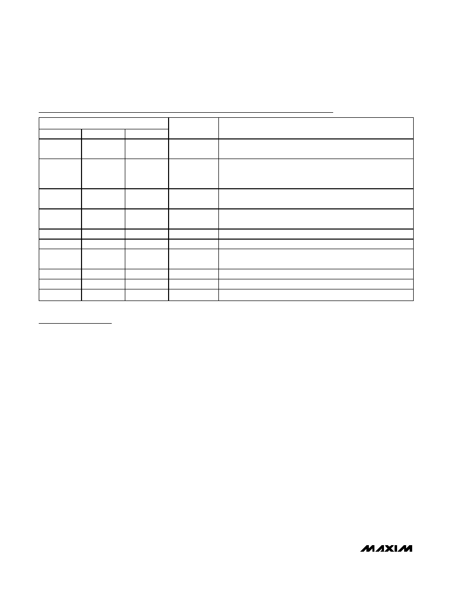
Pin Description
PIN
MAX4711
MAX4712
MAX4713
NAME
FUNCTION
1, 16, 9, 8
IN1, IN2, IN3,
IN4
Logic Inputs. Fault-protected to (V- + 12V).
2, 15, 10, 7
COM1,
COM2,
COM3, COM4
Analog Switch Common Terminals
3, 14, 11, 6
——
NC1, NC2,
NC3, NC4
Fault-Protected Analog Switch Normally Closed Terminals
—
3, 14, 11, 6
—
NO1, NO2,
NO3, NO4
Fault-Protected Analog Switch Normally Open Terminals
——
3, 6
NO1, NO4
Fault-Protected Analog Switch Normally Open Terminals
——
14, 11
NC2, NC3
Fault-Protected Analog Switch Normally Closed Terminals
44
4
V-
Negative Supply Voltage Input. Connect to GND for single-supply
operation.
55
5
GND
Ground
12
N.C.
No Connection. Not internally connected.
13
V+
Positive Supply Input
相关PDF资料 |
PDF描述 |
|---|---|
| VE-JTH-IX-F1 | CONVERTER MOD DC/DC 52V 75W |
| PIC16C67-04I/P | IC MCU OTP 8KX14 PWM 40DIP |
| VE-27K-IX-F3 | CONVERTER MOD DC/DC 40V 75W |
| MAX338CPE+ | IC MULTIPLEXER 8X1 16DIP |
| VE-2TP-IX-F4 | CONVERTER MOD DC/DC 13.8V 75W |
相关代理商/技术参数 |
参数描述 |
|---|---|
| MAX4712EUE+ | 功能描述:模拟开关 IC Quad SPST Analog Switch RoHS:否 制造商:Texas Instruments 开关数量:2 开关配置:SPDT 开启电阻(最大值):0.1 Ohms 切换电压(最大): 开启时间(最大值): 关闭时间(最大值): 工作电源电压:2.7 V to 4.5 V 最大工作温度:+ 85 C 安装风格:SMD/SMT 封装 / 箱体:DSBGA-16 |
| MAX4712EUE+T | 功能描述:模拟开关 IC Quad SPST Analog Switch RoHS:否 制造商:Texas Instruments 开关数量:2 开关配置:SPDT 开启电阻(最大值):0.1 Ohms 切换电压(最大): 开启时间(最大值): 关闭时间(最大值): 工作电源电压:2.7 V to 4.5 V 最大工作温度:+ 85 C 安装风格:SMD/SMT 封装 / 箱体:DSBGA-16 |
| MAX4712EUE-T | 功能描述:模拟开关 IC RoHS:否 制造商:Texas Instruments 开关数量:2 开关配置:SPDT 开启电阻(最大值):0.1 Ohms 切换电压(最大): 开启时间(最大值): 关闭时间(最大值): 工作电源电压:2.7 V to 4.5 V 最大工作温度:+ 85 C 安装风格:SMD/SMT 封装 / 箱体:DSBGA-16 |
| MAX4713CPE | 功能描述:模拟开关 IC RoHS:否 制造商:Texas Instruments 开关数量:2 开关配置:SPDT 开启电阻(最大值):0.1 Ohms 切换电压(最大): 开启时间(最大值): 关闭时间(最大值): 工作电源电压:2.7 V to 4.5 V 最大工作温度:+ 85 C 安装风格:SMD/SMT 封装 / 箱体:DSBGA-16 |
| MAX4713CSE | 功能描述:模拟开关 IC RoHS:否 制造商:Texas Instruments 开关数量:2 开关配置:SPDT 开启电阻(最大值):0.1 Ohms 切换电压(最大): 开启时间(最大值): 关闭时间(最大值): 工作电源电压:2.7 V to 4.5 V 最大工作温度:+ 85 C 安装风格:SMD/SMT 封装 / 箱体:DSBGA-16 |
发布紧急采购,3分钟左右您将得到回复。