- 您现在的位置:买卖IC网 > PDF目录1942 > MAX4719EUB+T (Maxim Integrated Products)IC SWITCH DUAL SPDT 10UMAX PDF资料下载
参数资料
| 型号: | MAX4719EUB+T |
| 厂商: | Maxim Integrated Products |
| 文件页数: | 4/11页 |
| 文件大小: | 0K |
| 描述: | IC SWITCH DUAL SPDT 10UMAX |
| 产品培训模块: | Lead (SnPb) Finish for COTS Obsolescence Mitigation Program |
| 标准包装: | 2,500 |
| 功能: | 开关 |
| 电路: | 2 x SPDT |
| 导通状态电阻: | 20 欧姆 |
| 电压电源: | 单电源 |
| 电压 - 电源,单路/双路(±): | 1.8 V ~ 5.5 V |
| 电流 - 电源: | 1µA |
| 工作温度: | -40°C ~ 85°C |
| 安装类型: | 表面贴装 |
| 封装/外壳: | 10-TFSOP,10-MSOP(0.118",3.00mm 宽) |
| 供应商设备封装: | 10-µMAX |
| 包装: | 带卷 (TR) |
MAX4719
20
, 300MHz Bandwidth, Dual SPDT Analog
Switch in UCSP
2
_______________________________________________________________________________________
ELECTRICAL CHARACTERISTICS—Single +3V Supply
(V+ = +2.7V to +3.6V, VIH = +1.4V, VIL = +0.5V, TA = TMIN to TMAX, unless otherwise noted. Typical values are at V+ = +3.0V,
TA = +25°C, unless otherwise noted.) (Notes 3, 4)
Stresses beyond those listed under “Absolute Maximum Ratings” may cause permanent damage to the device. These are stress ratings only, and functional
operation of the device at these or any other conditions beyond those indicated in the operational sections of the specifications is not implied. Exposure to
absolute maximum rating conditions for extended periods may affect device reliability.
(All Voltages Referenced to GND)
V+, IN_...................................................................-0.3V to +6.0V
COM_, NO_, NC_ (Note 1) ...........................-0.3V to (V+ + 0.3V)
Continuous Current COM_, NO_, NC_ ...........................±100mA
Peak Current COM_, NO_, NC_
(pulsed at 1ms, 10% duty cycle)................................±200mA
Continuous Power Dissipation (TA = +70°C)
10-Pin MAX (derate 5.6mW/°C above +70°C) ...........444mW
12-Bump UCSP (derate 11.4mW/°C above +70°C) ....909mW
ESD Method 3015.7 ...............................................................2kV
Operating Temperature Range ...........................-40°C to +85°C
Junction Temperature ......................................................+150°C
Storage Temperature Range .............................-65°C to +150°C
Lead Temperature (soldering, 10s) .................................+300°C
Bump Temperature (soldering) (Note 2)
Infrared (15s) ...............................................................+220°C
Vapor Phase (60s) .......................................................+215°C
Note 1: Signals on COM_, NO_, or NC_ exceeding V+ or GND are clamped by internal diodes. Limit forward-diode current to maxi-
mum current rating.
Note 2: This device is constructed using a unique set of packaging techniques that impose a limit on the thermal profile the device
can be exposed to during board level solder attach and rework. This limit permits only the use of the solder profiles recom-
mended in the industry standard specification, JEDEC 020A, paragraph 7.6, table 3 for IR/VPR and convection reflow.
Preheating is required. Hand or wave soldering is not allowed.
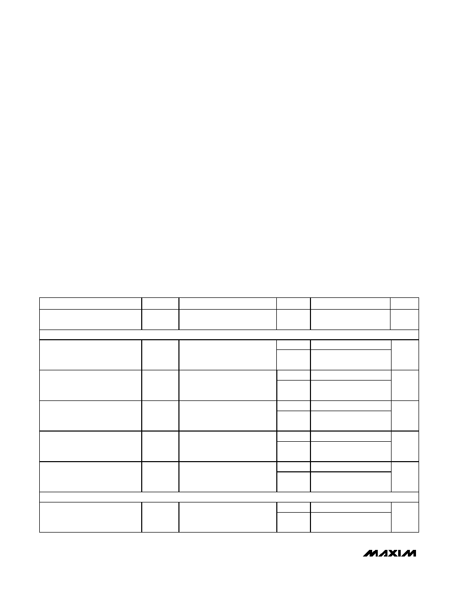
PARAMETER
SYMBOL
CONDITIONS
TA
MIN
TYP
MAX
UNITS
Analog Signal Range
VCOM_,
VNO_, VNC_
TMIN to
TMAX
0V+
V
ANALOG SWITCH
+25°C14
20
On-Resistance (Note 5)
RON
V+ = 2.7V, ICOM_ = 10mA;
VNO_ or VNC_ = 1.5V
TMIN to
TMAX
25
+25°C
0.15
0.4
On-Resistance Match Between
Channels (Notes 5, 6)
RON
V+ = 2.7V, ICOM_ = 10mA;
VNO_ or VNC_ = 1.5V
TMIN to
TMAX
0.5
+25°C
0.6
1.2
On-Resistance Flatness
(Note 7)
RFLAT(ON)
V+ = 2.7V, ICOM_ = 10mA;
VNO_ or VNC_ = 1.0V, 1.5V, 2.0V
TMIN to
TMAX
1.5
+25°C
-0.5
0.01
+0.5
NO_, NC_ Off-Leakage Current
(Note 8)
INO_(OFF),
INC_(OFF)
V+ = 3.6V, VCOM_ = 0.3V, 3.3V;
VNO_ or VNC_ = 3.3V, 0.3V
TMIN to
TMAX
-1
+1
nA
+25°C
-1
0.01
+1
COM_ On-Leakage Current
(Note 8)
ICOM_(ON)
V+ = 3.6V, VCOM_ = 0.3V, 3.3V;
VNO_ or VNC_ = 0.3V, 3.3V, or
floating
TMIN to
TMAX
-2
+2
nA
DYNAMIC CHARACTERISTICS
+25°C40
80
Turn-On Time
tON
VNO_, VNC_ = 1.5V;
RL = 300
, CL = 35pF, Figure 1
TMIN to
TMAX
100
ns
ABSOLUTE MAXIMUM RATINGS
相关PDF资料 |
PDF描述 |
|---|---|
| MAX4721EUA+ | IC SWITCH DUAL SPST 8UMAX |
| MAX4730ELT+T | IC SWITCH SPDT 6UDFN |
| MAX4732EUA+T | IC SWITCH DUAL SPST 8UMAX |
| MAX4734EGC+ | IC MULTIPLEXER 4X1 12QFN |
| MAX4736ETC+ | IC SWITCH DUAL SPDT 12TQFN |
相关代理商/技术参数 |
参数描述 |
|---|---|
| MAX471CPA | 功能描述:特殊用途放大器 RoHS:否 制造商:Texas Instruments 通道数量:Single 共模抑制比(最小值): 输入补偿电压: 工作电源电压:3 V to 5.5 V 电源电流:5 mA 最大功率耗散: 最大工作温度:+ 70 C 最小工作温度:- 40 C 安装风格:SMD/SMT 封装 / 箱体:QFN-20 封装:Reel |
| MAX471CSA | 功能描述:特殊用途放大器 RoHS:否 制造商:Texas Instruments 通道数量:Single 共模抑制比(最小值): 输入补偿电压: 工作电源电压:3 V to 5.5 V 电源电流:5 mA 最大功率耗散: 最大工作温度:+ 70 C 最小工作温度:- 40 C 安装风格:SMD/SMT 封装 / 箱体:QFN-20 封装:Reel |
| MAX471CSA+ | 功能描述:特殊用途放大器 RoHS:否 制造商:Texas Instruments 通道数量:Single 共模抑制比(最小值): 输入补偿电压: 工作电源电压:3 V to 5.5 V 电源电流:5 mA 最大功率耗散: 最大工作温度:+ 70 C 最小工作温度:- 40 C 安装风格:SMD/SMT 封装 / 箱体:QFN-20 封装:Reel |
| MAX471CSA+T | 功能描述:特殊用途放大器 RoHS:否 制造商:Texas Instruments 通道数量:Single 共模抑制比(最小值): 输入补偿电压: 工作电源电压:3 V to 5.5 V 电源电流:5 mA 最大功率耗散: 最大工作温度:+ 70 C 最小工作温度:- 40 C 安装风格:SMD/SMT 封装 / 箱体:QFN-20 封装:Reel |
| MAX471CSA-T | 功能描述:特殊用途放大器 RoHS:否 制造商:Texas Instruments 通道数量:Single 共模抑制比(最小值): 输入补偿电压: 工作电源电压:3 V to 5.5 V 电源电流:5 mA 最大功率耗散: 最大工作温度:+ 70 C 最小工作温度:- 40 C 安装风格:SMD/SMT 封装 / 箱体:QFN-20 封装:Reel |
发布紧急采购,3分钟左右您将得到回复。