- 您现在的位置:买卖IC网 > PDF目录3281 > MAX472CPA (Maxim Integrated Products)IC AMP CURR-SENSE HI-SIDE 8-DIP PDF资料下载
参数资料
| 型号: | MAX472CPA |
| 厂商: | Maxim Integrated Products |
| 文件页数: | 3/13页 |
| 文件大小: | 0K |
| 描述: | IC AMP CURR-SENSE HI-SIDE 8-DIP |
| 标准包装: | 50 |
| 放大器类型: | 电流检测 |
| 电路数: | 1 |
| 电流 - 输入偏压: | 20µA |
| 电压 - 输入偏移: | 120µV |
| 电流 - 电源: | 20µA |
| 电流 - 输出 / 通道: | 1.5mA |
| 电压 - 电源,单路/双路(±): | 3 V ~ 36 V |
| 工作温度: | 0°C ~ 70°C |
| 安装类型: | 通孔 |
| 封装/外壳: | 8-DIP(0.300",7.62mm) |
| 供应商设备封装: | 8-PDIP |
| 包装: | 管件 |
| 其它名称: | Q1142329 |
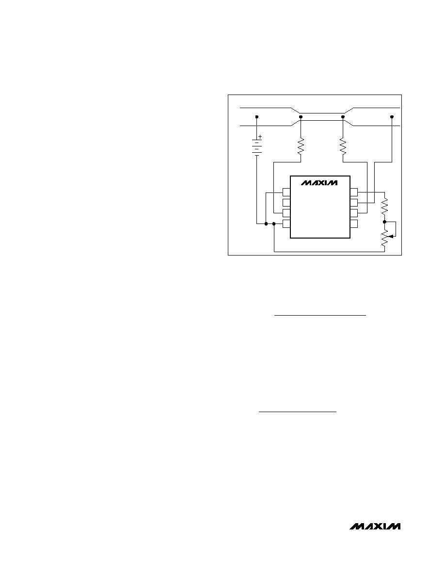
MAX471/MAX472
In Figure 6, assume the load current to be measured is
10A and that you have determined a 0.3 inch wide, 2
ounce copper to be appropriate. The resistivity of 0.1
inch wide, 2 ounce copper is 30m
/ft (see Note 4). For
10A you may want RSENSE = 5m
for a 50mV drop at
full scale. This resistor will require about 2 inches of 0.1
inch wide copper trace.
RG1 and RG2
Once RSENSE is chosen, RG1 and RG2 can be chosen
to define the current-gain ratio (RSENSE/RG). Choose
RG = RG1 = RG2 based on the following criteria:
a) 1
Input Resistance. The minimum RG value is lim-
ited by the 1
input resistance, and also by the out-
put current limitation (see below). As RG is reduced,
the input resistance becomes a larger portion of the
total gain-setting resistance. With RG = 50
, the
input resistance produces a 2% difference between
the expected and actual current-gain ratio. This is a
gain error that does not affect linearity and can be
removed by adjusting RG or ROUT.
b) Efficiency. As RG is reduced, IOUT gets larger for a
given load current. Power dissipated in ROUT is not
going to the load, and therefore reduces overall effi-
ciency. This is significant only when the sense cur-
rent is small.
c) Maximum Output Current Limitation. IOUT is limit-
ed to 1.5mA, requiring RG
≥ VSENSE / 1.5mA. For
VSENSE = 60mV, RG must be
≥ 40.
d) Headroom. The MAX472 requires a minimum of
1.5V between the lower of the voltage at RG1 or
RG2 (VRG_) and VOUT. As RG becomes larger, the
voltage drop across RG also becomes larger for a
given IOUT. This voltage drop further limits the maxi-
mum full-scale VOUT. Assuming the drop across
RSENSE is small and VCC is connected to either side
of RSENSE, VOUT (max) = VCC - (1.5V + IOUT (max) x
RG).
e) Output Offset Error at Low Load Currents. Large
RG values reduce IOUT for a given load current. As
IOUT gets smaller, the 2.5A max output offset-error
current becomes a larger part of the overall output
current. Keeping the gain high by choosing a low
value for RG minimizes this offset error.
f) Input Bias Current and Input Bias Current
Mismatching. The size of RG also affects the errors
introduced by the input bias and input bias mis-
matching currents. After selecting the ratio, check to
make sure RG is small enough that IB and IOS do
not add any appreciable errors. The full-scale error
is given by:
% Error =
(RG1 - RG2) x IB + IOS x RG x 100
IFS x RSENSE
where RG1 and RG2 are the gain resistors, IB is the
bias current, IOS is the bias-current mismatch, IFS is the
full-scale current, and RSENSE is the sense resistor.
Assuming a 5A load current, 10m
RSENSE, and 100
RG, the current-gain ratio is 100A/A, yielding a full-
scale IOUT of 500A. Using the maximum values for IB
(20A) and IOS (2A), and 1% resistors for RG1 and
RG2 (RG1 - RG2 = 2
), the worst-case error at full
scale calculates to:
2
x 20A + 100 x 2A
= 0.48%
5m
x 5A
The error may be reduced by: a) better matching of
RG1 and RG2, b) increasing RSENSE, or c) decreasing
RG.
Current-Sense Adjustment
(Resistor Range, Output Adjust)
Choose ROUT after selecting RSENSE, RG1, and RG2.
Choose ROUT to obtain the full-scale voltage you
Precision, High-Side
Current-Sense Amplifiers
10
______________________________________________________________________________________
Note 4: Printed Circuit Design, by Gerald L. Ginsberg; McGraw-Hill, Inc.; page 185.
3V
TO
36V
RSENSE
1
2
3
4
8
7
6
5
MAX472
0.1" COPPER
0.3" COPPER
RG2
RG1
1.5k
1k
POWER
SOURCE
OR
BATTERY
TO LOAD/CHARGER
RG1
N.C.
SHDN
SIGN
OUT
VCC
GND
RG2
Figure 6. MAX472 Connections Showing Use of PC Board
Trace
相关PDF资料 |
PDF描述 |
|---|---|
| MAX479CPD | IC OPAMP SNGL SUP QUAD 14-DIP |
| RMCF2010JT820R | RES 820 OHM 3/4W 5% 2010 SMD |
| MAX475CSD | IC OPAMP QUAD 10MHZ 14-SOIC |
| 2-534237-3 | CONN RCPT 25POS .100 VERT |
| MAX474CSA | IC OPAMP DUAL 10MHZ 8-SOIC |
相关代理商/技术参数 |
参数描述 |
|---|---|
| MAX472CPA+ | 功能描述:特殊用途放大器 RoHS:否 制造商:Texas Instruments 通道数量:Single 共模抑制比(最小值): 输入补偿电压: 工作电源电压:3 V to 5.5 V 电源电流:5 mA 最大功率耗散: 最大工作温度:+ 70 C 最小工作温度:- 40 C 安装风格:SMD/SMT 封装 / 箱体:QFN-20 封装:Reel |
| MAX472CSA | 功能描述:特殊用途放大器 RoHS:否 制造商:Texas Instruments 通道数量:Single 共模抑制比(最小值): 输入补偿电压: 工作电源电压:3 V to 5.5 V 电源电流:5 mA 最大功率耗散: 最大工作温度:+ 70 C 最小工作温度:- 40 C 安装风格:SMD/SMT 封装 / 箱体:QFN-20 封装:Reel |
| MAX472CSA+ | 功能描述:特殊用途放大器 RoHS:否 制造商:Texas Instruments 通道数量:Single 共模抑制比(最小值): 输入补偿电压: 工作电源电压:3 V to 5.5 V 电源电流:5 mA 最大功率耗散: 最大工作温度:+ 70 C 最小工作温度:- 40 C 安装风格:SMD/SMT 封装 / 箱体:QFN-20 封装:Reel |
| MAX472CSA+T | 功能描述:特殊用途放大器 RoHS:否 制造商:Texas Instruments 通道数量:Single 共模抑制比(最小值): 输入补偿电压: 工作电源电压:3 V to 5.5 V 电源电流:5 mA 最大功率耗散: 最大工作温度:+ 70 C 最小工作温度:- 40 C 安装风格:SMD/SMT 封装 / 箱体:QFN-20 封装:Reel |
| MAX472CSA-T | 功能描述:特殊用途放大器 RoHS:否 制造商:Texas Instruments 通道数量:Single 共模抑制比(最小值): 输入补偿电压: 工作电源电压:3 V to 5.5 V 电源电流:5 mA 最大功率耗散: 最大工作温度:+ 70 C 最小工作温度:- 40 C 安装风格:SMD/SMT 封装 / 箱体:QFN-20 封装:Reel |
发布紧急采购,3分钟左右您将得到回复。