- 您现在的位置:买卖IC网 > PDF目录11331 > MAX4736EGC+ (Maxim Integrated Products)IC SWITCH DUAL SPDT 12QFN PDF资料下载
参数资料
| 型号: | MAX4736EGC+ |
| 厂商: | Maxim Integrated Products |
| 文件页数: | 8/10页 |
| 文件大小: | 0K |
| 描述: | IC SWITCH DUAL SPDT 12QFN |
| 产品培训模块: | Lead (SnPb) Finish for COTS Obsolescence Mitigation Program Low Voltage Analog Switches Overview |
| 标准包装: | 100 |
| 功能: | 开关 |
| 电路: | 2 x SPDT |
| 导通状态电阻: | 800 毫欧 |
| 电压电源: | 单电源 |
| 电压 - 电源,单路/双路(±): | 1.6 V ~ 4.2 V |
| 电流 - 电源: | 1µA |
| 工作温度: | -40°C ~ 85°C |
| 安装类型: | 表面贴装 |
| 封装/外壳: | 12-VFQFN 裸露焊盘 |
| 供应商设备封装: | 12-QFN-EP(3x3) |
| 包装: | 管件 |
Detailed Description
The MAX4736 is a low 0.8Ω max (at V+ = 2.7V) onresis-
tance, low-voltage, dual SPDT analog switch that oper-
ates from a 1.6V to 4.2V single supply. CMOS switch
construction allows switching analog signals that range
from GND to V+.
When powered from a 2.7V supply, the 0.8Ω max RON
allows high continuous currents to be switched in a variety
of applications.
Applications Information
Proper power-supply sequencing is recommended for all
CMOS devices. Do not exceed the absolute maximum
ratings; stresses beyond the listed ratings can cause per-
manent damage to the devices. Always sequence V+ on
first, followed by NO_, NC_, or COM_.
Although it is not required, power-supply bypassing
improves noise margin and prevents switching noise
propagation from the V+ supply to other components. A
0.1μF capacitor, connected from V+ to GND, is adequate
for most applications.
Logic Inputs
The MAX4736 logic inputs can be driven up to 3.6V,
regardless of the supply voltage. For example, with a 1.8V
supply, IN_ can be driven low to GND and high to 3.6V.
Driving IN_ rail-to-rail minimizes power consumption.
Analog Signal Levels
Analog signals that range over the entire supply voltage
(V+ to GND) can be passed with very little change in
onresistance (see Typical Operating Characteristics). The
switches are bidirectional, so the NO_, NC_, and COM_
pins can be used as either inputs or outputs.
Layout
High-speed switches require proper layout and design
procedures for optimum performance. Reduce stray induc-
tance and capacitance by keeping traces short and wide.
Ensure that bypass capacitors are as close to the device
as possible. Use large ground planes where possible.
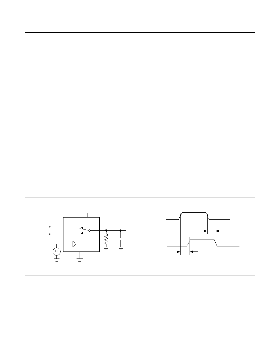
Figure 1. Switching Time
tr < 5ns
tf < 5ns
50%
0
VIN_ = VIH + 0.5V
tOFF
0
0.9 x V0UT
0.9 x VOUT
tON
VOUT
SWITCH
OUTPUT
LOGIC
INPUT
LOGIC INPUT WAVEFORMS INVERTED FOR SWITCHES
THAT HAVE THE OPPOSITE LOGIC SENSE.
MAX4736
LOGIC
INPUT
RL
GND
CL INCLUDES FIXTURE AND STRAY CAPACITANCE.
NO_ or NC_
IN_
NC_ or NO_
VOUT
V+
CL
VIN
COM_
MAX4736
0.6Ω, Low-Voltage, Single-Supply, Dual SPDT
Analog Switch
www.maximintegrated.com
Maxim Integrated │ 7
Test Circuits/Timing Diagrams
相关PDF资料 |
PDF描述 |
|---|---|
| PIC16LC66-04I/SP | IC MCU OTP 8KX14 PWM 28DIP |
| MAX4618EUE+ | IC MULTIPLEXER DUAL 4X1 16TSSOP |
| PIC32MX764F128HT-I/MR | IC PIC MCU 128KBIT FLASH 64QFN |
| PIC24FJ256DA106T-I/MR | MCU 16BIT 256K FLASH 64-QFN |
| PIC24HJ64GP510A-E/PF | IC PIC MCU FLASH 64KB 100-TQFP |
相关代理商/技术参数 |
参数描述 |
|---|---|
| MAX4736EGC+ | 功能描述:模拟开关 IC .6Ohm Dual SPST Analog Switch RoHS:否 制造商:Texas Instruments 开关数量:2 开关配置:SPDT 开启电阻(最大值):0.1 Ohms 切换电压(最大): 开启时间(最大值): 关闭时间(最大值): 工作电源电压:2.7 V to 4.5 V 最大工作温度:+ 85 C 安装风格:SMD/SMT 封装 / 箱体:DSBGA-16 |
| MAX4736EGC+GH7 | 功能描述:模拟开关 IC 0.8ohm Low-Voltage Single-Supply Dual SPDT Analog Switch RoHS:否 制造商:Texas Instruments 开关数量:2 开关配置:SPDT 开启电阻(最大值):0.1 Ohms 切换电压(最大): 开启时间(最大值): 关闭时间(最大值): 工作电源电压:2.7 V to 4.5 V 最大工作温度:+ 85 C 安装风格:SMD/SMT 封装 / 箱体:DSBGA-16 |
| MAX4736EGC+T | 功能描述:模拟开关 IC .6Ohm Dual SPST Analog Switch RoHS:否 制造商:Texas Instruments 开关数量:2 开关配置:SPDT 开启电阻(最大值):0.1 Ohms 切换电压(最大): 开启时间(最大值): 关闭时间(最大值): 工作电源电压:2.7 V to 4.5 V 最大工作温度:+ 85 C 安装风格:SMD/SMT 封装 / 箱体:DSBGA-16 |
| MAX4736EGC+TGH7 | 功能描述:模拟开关 IC 0.6 Ohm Low-Voltage Single-Supply Dual SPDT Analog Switch RoHS:否 制造商:Texas Instruments 开关数量:2 开关配置:SPDT 开启电阻(最大值):0.1 Ohms 切换电压(最大): 开启时间(最大值): 关闭时间(最大值): 工作电源电压:2.7 V to 4.5 V 最大工作温度:+ 85 C 安装风格:SMD/SMT 封装 / 箱体:DSBGA-16 |
| MAX4736EGC-T | 功能描述:模拟开关 IC RoHS:否 制造商:Texas Instruments 开关数量:2 开关配置:SPDT 开启电阻(最大值):0.1 Ohms 切换电压(最大): 开启时间(最大值): 关闭时间(最大值): 工作电源电压:2.7 V to 4.5 V 最大工作温度:+ 85 C 安装风格:SMD/SMT 封装 / 箱体:DSBGA-16 |
发布紧急采购,3分钟左右您将得到回复。