- 您现在的位置:买卖IC网 > PDF目录385531 > MAX477 (Maxim Integrated Products, Inc.) 300MHz High-Speed Op Amp(300MHz 高速运算放大器) PDF资料下载
参数资料
| 型号: | MAX477 |
| 厂商: | Maxim Integrated Products, Inc. |
| 英文描述: | 300MHz High-Speed Op Amp(300MHz 高速运算放大器) |
| 中文描述: | 300MHz、高速运算放大器 |
| 文件页数: | 2/12页 |
| 文件大小: | 176K |
| 代理商: | MAX477 |
M
300MHz High-S peed Op Amp
2
_______________________________________________________________________________________
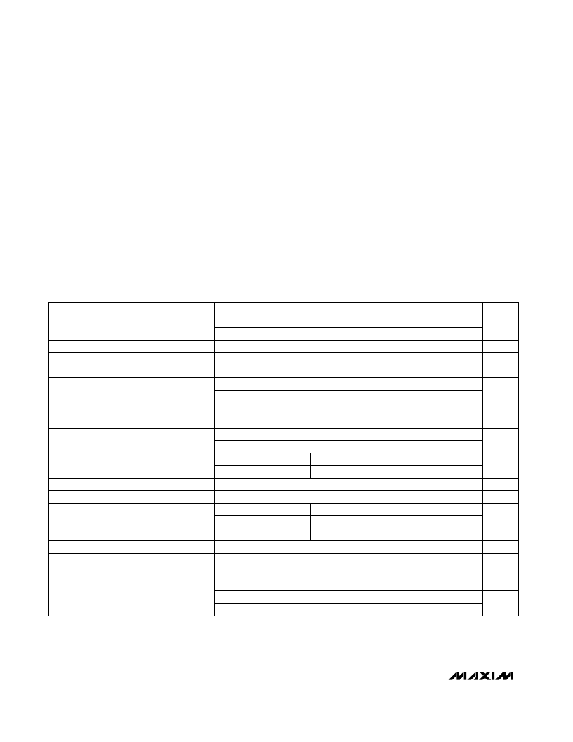
ABSOLUTE MAXIMUM RATINGS
Supply Voltage (V
CC
to V
EE
)..................................................13V
Differential Input Voltage..................(V
CC
+ 0.3V) to (V
EE
- 0.3V)
Common-Mode Input Voltage..........(V
CC
+ 0.3V) to (V
EE
- 0.3V)
Output Short-Circuit Duration to GND........................Continuous
Continuous Power Dissipation (T
A
= +70°C)
Plastic DIP (derate 9.09mW/°C above +70°C)..............727mW
SO (derate 5.88mW/°C above +70°C)..........................471mW
μMAX (derate 4.1mW/°C above +70°C) .......................330mW
CERDIP (derate 8.00mW/°C above +70°C)..................640mW
DC ELECTRICAL CHARACTERISTICS
(V
CC
= +5V, V
EE
= -5V, V
OUT
= 0V, R
L
=
∞
, T
A
= T
MIN
to T
MAX,
unless otherwise noted. Typical values are at T
A
= +25°C.)
Stresses beyond those listed under “Absolute Maximum Ratings” may cause permanent damage to the device. These are stress ratings only, and functional
operation of the device at these or any other conditions beyond those indicated in the operational sections of the specifications is not implied. Exposure to
absolute maximum rating conditions for extended periods may affect device reliability.
Operating Temperature Ranges
MAX477E_A......................................................-40°C to +85°C
MAX477MJ A ...................................................-55°C to +125°C
Storage Temperature Range.............................-65°C to +160°C
Lead Temperature (soldering, 10sec) .............................+300°C
T
A
= +25°C
T
A
= T
MIN
to T
MAX
MAX477MJ A, T
A
= T
MIN
to T
MAX
MAX477E_A, T
A
= T
MIN
to T
MAX
T
A
= +25°C
V
OUT
= 0, f = DC
T
A
= T
MIN
to T
MAX
T
A
= +25°C
T
A
= T
MIN
to T
MAX
T
A
= +25°C
Short to ground
Either input
T
A
= +25°C
T
A
= T
MIN
to T
MAX
T
A
= +25°C
CONDITIONS
mA
14
I
SY
Quiescent Supply Current
12
mA
8
10
0.1
R
OUT
Open-Loop Output Resistance
mA
150
I
SC
Short-Circuit Output Current
V
±2.5
70
V
OUT
Output Voltage Swing
±3.0
±3.5
±3.9
0.5
2.0
3.0
V
±2.5
70
V
CM
Common-Mode Input Voltage
Range
±3.0
±3.5
M
1
R
IN(DM)
Differential-Mode Input
Resistance
μV/°C
2
1
TCV
OS
Input Offset-Voltage Drift
3
UNITS
MIN
TYP
MAX
SYMBOL
PARAMETER
T
A
= +25°C
T
A
= T
MIN
to T
MAX
0.2
0.5
2.0
dB
60
70
55
CMRR
Common-Mode Rejection Ratio
90
V
S
= ±4.5V to ±5.5V
V
OUT
= ±2.0V, V
CM
= 0V, R
L
= 50
dB
dB
PSRR
A
VOL
Power-Supply Rejection Ratio
Open-Loop Voltage Gain
85
65
T
A
= -40 °C to +85 °C
mA
100
I
OUT
Minimum Output Current
Input Offset Voltage
V
OS
mV
μA
5.0
I
B
Input Bias Current
Input Offset Current
I
OS
μA
V
CM
= ±3V
V
CM
= ±2.5V
R
L
=
∞
R
L
= 100
R
L
= 50
T
A
= T
MIN
to T
MAX
相关PDF资料 |
PDF描述 |
|---|---|
| MAX4789EUK | 200mA/250mA/300mA Current-Limit Switches |
| MAX4789EUS | 200mA/250mA/300mA Current-Limit Switches |
| MAX4793EUK | 200mA/250mA/300mA Current-Limit Switches |
| MAX4793EUS | 200mA/250mA/300mA Current-Limit Switches |
| MAX4794EUS | 200mA/250mA/300mA Current-Limit Switches |
相关代理商/技术参数 |
参数描述 |
|---|---|
| MAX4772ETT+T | 功能描述:电源开关 IC - 配电 200mA/500mA Select Current-Limit Switch RoHS:否 制造商:Exar 输出端数量:1 开启电阻(最大值):85 mOhms 开启时间(最大值):400 us 关闭时间(最大值):20 us 工作电源电压:3.2 V to 6.5 V 电源电流(最大值): 最大工作温度:+ 85 C 安装风格:SMD/SMT 封装 / 箱体:SOT-23-5 |
| MAX4772ETT-T | 功能描述:电源开关 IC - 配电 RoHS:否 制造商:Exar 输出端数量:1 开启电阻(最大值):85 mOhms 开启时间(最大值):400 us 关闭时间(最大值):20 us 工作电源电压:3.2 V to 6.5 V 电源电流(最大值): 最大工作温度:+ 85 C 安装风格:SMD/SMT 封装 / 箱体:SOT-23-5 |
| MAX4772EUT | 制造商:Maxim Integrated Products 功能描述:- Cut Tape Product |
| MAX4772EUT+ | 制造商:Maxim Integrated Products 功能描述:- Cut Tape Product |
| MAX4772EUT+T | 功能描述:电源开关 IC - 配电 200mA/500mA Select Current-Limit Switch RoHS:否 制造商:Exar 输出端数量:1 开启电阻(最大值):85 mOhms 开启时间(最大值):400 us 关闭时间(最大值):20 us 工作电源电压:3.2 V to 6.5 V 电源电流(最大值): 最大工作温度:+ 85 C 安装风格:SMD/SMT 封装 / 箱体:SOT-23-5 |
发布紧急采购,3分钟左右您将得到回复。