- 您现在的位置:买卖IC网 > PDF目录11155 > MAX4796EUK+T (Maxim Integrated Products)IC SWITCH 1X1 SOT23-5 PDF资料下载
参数资料
| 型号: | MAX4796EUK+T |
| 厂商: | Maxim Integrated Products |
| 文件页数: | 2/9页 |
| 文件大小: | 0K |
| 描述: | IC SWITCH 1X1 SOT23-5 |
| 产品培训模块: | Lead (SnPb) Finish for COTS Obsolescence Mitigation Program |
| 标准包装: | 2,500 |
| 功能: | 开关 |
| 电路: | 1 x 1:1 |
| 导通状态电阻: | 400 毫欧 |
| 电流 - 电源: | 125µA |
| 工作温度: | -40°C ~ 85°C |
| 安装类型: | 表面贴装 |
| 封装/外壳: | SC-74A,SOT-753 |
| 供应商设备封装: | SOT-23-5 |
| 包装: | 带卷 (TR) |
MAX4795–MAX4798
450mA/500mA Current-Limit Switches
2
_______________________________________________________________________________________
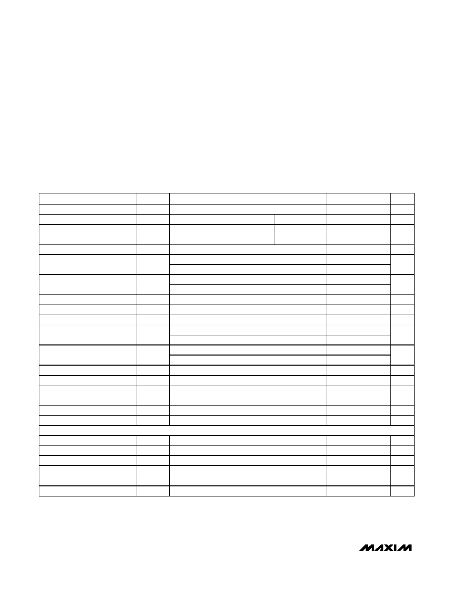
ABSOLUTE MAXIMUM RATINGS
ELECTRICAL CHARACTERISTICS
(VIN = +2.0V to +4.5V, TA = -40°C to +85°C, unless otherwise noted. Typical values are at VIN = 3.3V, TA = +25°C.) (Note 1)
Stresses beyond those listed under “Absolute Maximum Ratings” may cause permanent damage to the device. These are stress ratings only, and functional
operation of the device at these or any other conditions beyond those indicated in the operational sections of the specifications is not implied. Exposure to
absolute maximum rating conditions for extended periods may affect device reliability.
Note 1: All parts are 100% tested at +25°C. Electrical limits across the full temperature range are guaranteed by design and correlation.
Note 2: Latch-off current does not include the current flowing into FLAG.
Note 3: TDFN packages are guaranteed by design.
Note 4: The on-time is defined as the time taken for the current through the switch to go from 0mA to full load. The off-time is defined as
the time taken for the current through the switch to go from full load to 0mA.
Note 5: Retry time is typically 15 times the blanking time.
IN, ON, FLAG, OUT to GND .....................................-0.3V to +6V
OUT Short Circuit to GND .................................Internally Limited
Continuous Power Dissipation (TA = +70°C)
5-Pin SOT23 (derate 7.1mW/°C above +70°C)............571mW
6-Pin TDFN (derate 24.4mW/°C above +70°C) .........1951mW
Operating Temperature Range ...........................-40°C to +85°C
Junction Temperature ......................................................+150°C
Storage Temperature Range .............................-65°C to +150°C
Lead Temperature (soldering, 10s) .................................+300°C
PARAMETER
SYMBOL
CONDITIONS
MIN
TYP
MAX
UNITS
Operating Voltage
VIN
2.0
4.5
V
Quiescent Current
IQ
VON = VIN, IOUT = 0, switch on
VIN = +3.3V
80
125
A
Latch-Off Current
ILATCH
VON = VIN, after an overcurrent
fault (MAX4795/MAX4797) (Note 2)
VIN = +3.3V
6
10
A
Shutdown Current
ISHDN
VON = 0V
0.03
1
A
MAX4795/MAX4796, VIN = 3.3V, VOUT = GND
450
720
Forward Current Limit
MAX4797/MAX4798, VIN = 3.3V, VOUT = GND
500
800
mA
MAX4795/MAX4796
720
Reverse Current Limit
MAX4797/MAX4798
800
mA
ON Input Leakage
-1
+1
A
Shutdown Forward Leakage
VON = 0V, VOUT = 0V
0.01
1
A
Shutdown Reverse Leakage
VON = 0V, VIN = 2V, VOUT = 4.5V
1
A
MAX4795/MAX4796, ILOAD = 100mA
0.2
0.4
On-Resistance (Note 3)
RON
MAX4797/MAX4798, ILOAD = 100mA
0.18
0.36
VIN = +2V to +3.6V
1.4
ON Input Logic High Voltage
VIH
VIN > 3.6V
2
V
ON Input Logic Low Voltage
VIL
0.5
V
FLAG Output Logic Low Voltage
ISINK = 1mA
0.4
V
FLAG Output High Leakage
Current
VIN = VFLAG = VON = 4.5V
1
A
Thermal Shutdown
150
°C
Thermal-Shutdown Hysteresis
15
°C
DYNAMIC
Turn-On Time
VON from low to high; IOUT = 10mA, CL = 0.1F (Note 4)
120
s
Turn-Off Time
VON from high to low; IOUT = 10mA, CL = 0.1F (Note 4)
100
ns
Blanking Time
tBLANK
Overcurrent fault; Figures 2, 3
14
60
ms
Short-Circuit Current-Limit
Response Time
VON = VIN, short circuit applied to OUT
5
s
Retry Time
tRETRY
MAX4796/MAX4798, Figure 2 (Note 5)
210
900
ms
相关PDF资料 |
PDF描述 |
|---|---|
| C8051F567-IQ | IC 8051 MCU 16K FLASH 32-QFP |
| MAX4795EUK+T | IC SWITCH 1X1 SOT23-5 |
| MAX4773EUT+T | IC SWITCH 1X1 SOT23-6 |
| MAX4772ETT+T | IC SWITCH 1X1 6TDFN |
| MAX4932EBC+T | IC MULTIPLEXER DUAL 3X1 12UCSP |
相关代理商/技术参数 |
参数描述 |
|---|---|
| MAX4797ETT+T | 功能描述:电源开关 IC - 配电 450mA/500mA Current Limit Switch RoHS:否 制造商:Exar 输出端数量:1 开启电阻(最大值):85 mOhms 开启时间(最大值):400 us 关闭时间(最大值):20 us 工作电源电压:3.2 V to 6.5 V 电源电流(最大值): 最大工作温度:+ 85 C 安装风格:SMD/SMT 封装 / 箱体:SOT-23-5 |
| MAX4797ETT-T | 功能描述:电源开关 IC - 配电 RoHS:否 制造商:Exar 输出端数量:1 开启电阻(最大值):85 mOhms 开启时间(最大值):400 us 关闭时间(最大值):20 us 工作电源电压:3.2 V to 6.5 V 电源电流(最大值): 最大工作温度:+ 85 C 安装风格:SMD/SMT 封装 / 箱体:SOT-23-5 |
| MAX4797EUK | 制造商:Maxim Integrated Products 功能描述:- Cut Tape Product |
| MAX4797EUK-T | 功能描述:电源开关 IC - 配电 RoHS:否 制造商:Exar 输出端数量:1 开启电阻(最大值):85 mOhms 开启时间(最大值):400 us 关闭时间(最大值):20 us 工作电源电压:3.2 V to 6.5 V 电源电流(最大值): 最大工作温度:+ 85 C 安装风格:SMD/SMT 封装 / 箱体:SOT-23-5 |
| MAX4798ETT+T | 功能描述:电源开关 IC - 配电 450mA/500mA Current Limit Switch RoHS:否 制造商:Exar 输出端数量:1 开启电阻(最大值):85 mOhms 开启时间(最大值):400 us 关闭时间(最大值):20 us 工作电源电压:3.2 V to 6.5 V 电源电流(最大值): 最大工作温度:+ 85 C 安装风格:SMD/SMT 封装 / 箱体:SOT-23-5 |
发布紧急采购,3分钟左右您将得到回复。