- 您现在的位置:买卖IC网 > PDF目录21936 > MAX4810CTN+ (Maxim Integrated)IC DIGITAL PULSER DL 56TQFN-EP PDF资料下载
参数资料
| 型号: | MAX4810CTN+ |
| 厂商: | Maxim Integrated |
| 文件页数: | 9/20页 |
| 文件大小: | 0K |
| 描述: | IC DIGITAL PULSER DL 56TQFN-EP |
| 产品培训模块: | Lead (SnPb) Finish for COTS Obsolescence Mitigation Program |
| 标准包装: | 43 |
| 类型: | 线性 - 单极,双极 |
| 电源电压: | 4.75 V ~ 12.6 V |
| 电流 - 电源: | 36mA |
| 电流 - 输出(最大): | 1.3A |
| 输出类型: | 电压和电流 |
| 工作温度: | 0°C ~ 70°C |
| 封装/外壳: | 56-WFQFN 裸露焊盘 |
| 供应商设备封装: | 56-TQFN-EP(7x7) |
| 包装: | 管件 |
�� �
�
�Dual,� Unipolar/Bipolar,� High-Voltage�
�Digital� Pulsers�
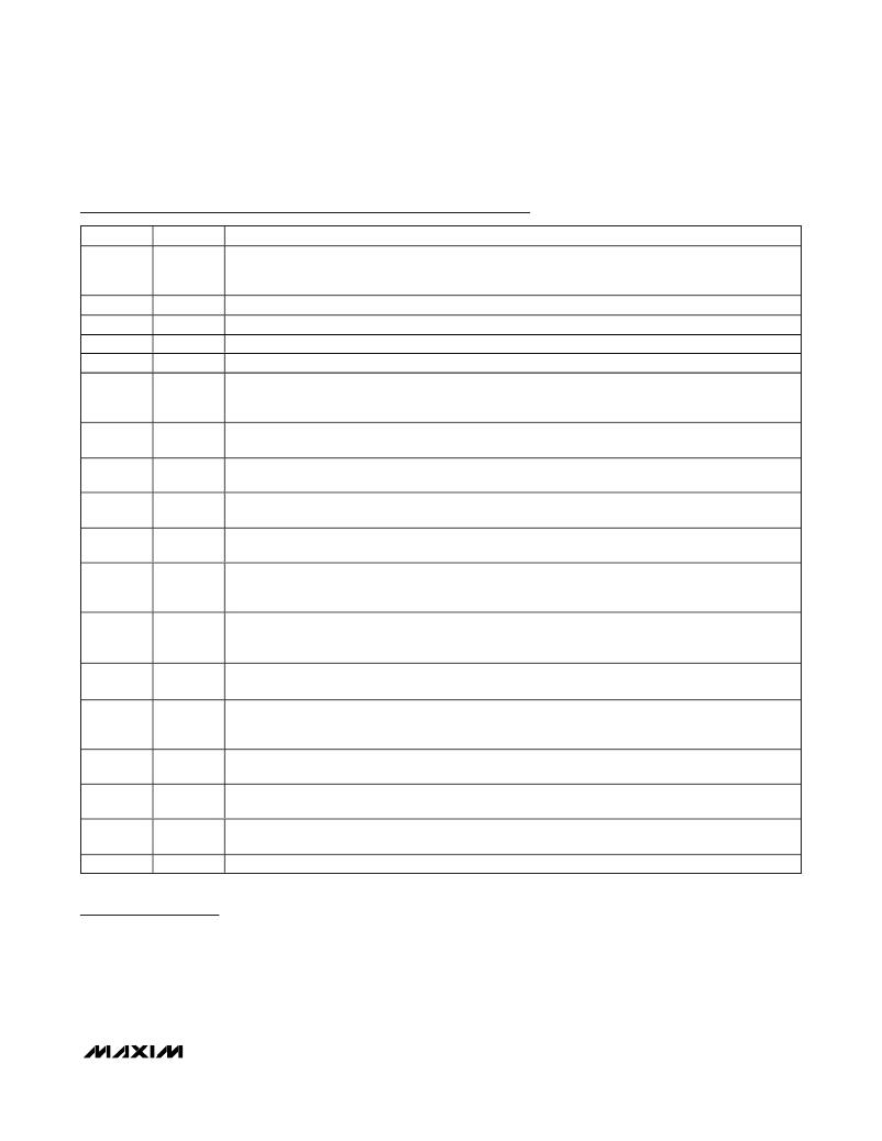
�Pin� Description� (continued)�
�PIN�
�31,� 32�
�34�
�35�
�37�
�38�
�40,� 41�
�42�
�43�
�46�
�47�
�48�
�49�
�50�
�51�
�52�
�53�
�56�
�—�
�NAME�
�V� NN2�
�ON2�
�OCN2�
�OCP2�
�OP2�
�V� PP2�
�C� GP2�
�C� DP2�
�C� GC2�
�C� DC2�
�V� EE2�
�V� DD�
�V� SS�
�V� EE1�
�C� DC1�
�C� GC1�
�C� DP1�
�EP�
�FUNCTION�
�Channel� 2� High-Side� Negative� Supply� Voltage� Input.� Bypass� V� NN2� to� GND� with� a� 0.1μF� as� close� as�
�possible� to� the� device.� See� the� Power� Supplies� and� Bypassing� section.� Depending� on� the� output,�
�additional� bypassing� may� be� required.�
�Channel� 2� Low-Side� Drain� Output�
�Channel� 2� Low-Side� Clamp� Output�
�Channel� 2� High-Side� Clamp� Output�
�Channel� 2� High-Side� Drain� Output�
�Channel� 2� High-Side� Supply� Voltage� Input.� Bypass� V� PP2� to� GND� with� a� 0.1μF� as� close� as� possible� to� the�
�device.� See� the� Power� Supplies� and� Bypassing� section.� Depending� on� the� output,� additional� bypassing�
�may� be� required.�
�Channel� 2� High-Side� Gate� Input.� Connect� a� 1nF� to� 10nF� capacitor� between� C� DP2� and� C� GP2� as� close� as�
�possible� to� the� device.�
�Channel� 2� High-Side� Driver� Output.� Connect� a� 1nF� to� 10nF� capacitor� between� C� DP2� and� C� GP2� as� close�
�as� possible� to� the� device.�
�Channel� 2� High-Side� Clamp� Gate� Input.� Connect� a� 1nF� to� 10nF� capacitor� between� C� DC2� and� C� GC2� as�
�close� as� possible� to� the� device.�
�Channel� 2� High-Side� Clamp� Driver� Output.� Connect� a� 1nF� to� 10nF� capacitor� between� C� DC2� and� C� GC2� as�
�close� as� possible� to� the� device.�
�Channel� 2� Negative� Supply� Input.� |V� EE2� |� ≤� V� CC2� .� Gate� Drive� Supply� Voltage� for� the� OCP� clamp.� Bypass�
�V� EE2� to� GND� with� a� 0.1μF� as� close� as� possible� to� the� device.� See� the� Power� Supplies� and� Bypassing�
�section.� Depending� on� the� output,� additional� bypassing� may� be� required.�
�Logic� Supply� Voltage� Input.� Bypass� V� DD� to� GND� with� a� 0.1μF� as� close� as� possible� to� the� device.� See� the�
�Power� Supplies� and� Bypassing� section.� Depending� on� the� output,� additional� bypassing� may� be�
�required.�
�Substrate� Voltage.� Connect� V� SS� to� a� voltage� equal� to� or� more� negative� than� the� more� negative� of� V� NN1� or�
�V� NN2� .�
�Channel� 1� Negative� Supply� Input.� |V� EE1� |� ≤� V� CC1� .� Gate� Drive� Supply� Voltage� for� the� OCP� clamp.� Bypass�
�V� EE1� to� GND� with� a� 0.1μF� as� close� as� possible� to� the� device.� See� the� Power� Supplies� and� Bypassing�
�section.� Depending� on� the� output,� additional� bypassing� may� be� required.�
�Channel� 1� High-Side� Clamp� Driver� Output.� Connect� a� 1nF� to� 10nF� capacitor� between� C� DC1� and� C� GC1� as�
�close� as� possible� to� the� device.�
�Channel� 1� High-Side� Clamp� Gate� Input.� Connect� a� 1nF� to� 10nF� capacitor� between� C� DC1� and� C� GC1� as�
�close� as� possible� to� the� device.�
�Channel� 1� High-Side� Driver� Output.� Connect� a� 1nF� to� 10nF� capacitor� between� C� DP1� and� C� GP1� as� close�
�as� possible� to� the� device.�
�Exposed� Pad.� EP� must� be� connected� to� V� SS� .� Do� not� use� EP� as� the� only� V� SS� connection� for� the� device.�
�Detailed� Description�
�The� MAX4810/MAX4811/MAX4812� are� dual� high-volt-�
�age,� high-speed� pulsers� that� can� be� independently�
�configured� for� either� unipolar� or� bipolar� pulse� outputs.�
�These� devices� have� independent� logic� inputs� for� full�
�pulse� control� and� independent� active� clamps.� The�
�clamp� input,� INC_,� can� be� set� high� to� activate� the�
�clamp� automatically� when� the� device� is� not� pulsing� to�
�the� positive� or� negative� high-voltage� supplies.�
�Logic� Inputs� (INP_,� INN_,� INC_,� EN_,� SHDN� )�
�The� MAX4810/MAX4811/MAX4812� have� a� total� of� nine�
�logic� input� signals.� SHDN� controls� power-up� and� power-�
�down� of� the� device.� There� are� two� sets� of� INP_,� INN_,�
�INC_,� and� EN_� signals:� one� for� each� channel.� INP_�
�_______________________________________________________________________________________�
�9�
�相关PDF资料 |
PDF描述 |
|---|---|
| M5010045 | MODULE POWER 100A 1200V AC SW |
| M5010042 | MODULE POWER 100A 600V AC SWITCH |
| B-60-5 | CORD PATCH BANANA PLUG 60" GREEN |
| GLA.02 | ANT GPS SMT CERAMIC LOOP |
| AFL000-00E | SWITCH MAGNETIC DIG 1.3V 8MSOP |
相关代理商/技术参数 |
参数描述 |
|---|---|
| MAX4810CTN+ | 功能描述:计时器和支持产品 Dual Uni/Bi-polar Digital Pulser RoHS:否 制造商:Micrel 类型:Standard 封装 / 箱体:SOT-23 内部定时器数量:1 电源电压-最大:18 V 电源电压-最小:2.7 V 最大功率耗散: 最大工作温度:+ 85 C 最小工作温度:- 40 C 封装:Reel |
| MAX4810CTN+T | 功能描述:计时器和支持产品 Dual Uni/Bi-polar Digital Pulser RoHS:否 制造商:Micrel 类型:Standard 封装 / 箱体:SOT-23 内部定时器数量:1 电源电压-最大:18 V 电源电压-最小:2.7 V 最大功率耗散: 最大工作温度:+ 85 C 最小工作温度:- 40 C 封装:Reel |
| MAX4810EVKIT+ | 功能描述:时钟和定时器开发工具 MAX4810/11/12 Eval Kit RoHS:否 制造商:Texas Instruments 产品:Evaluation Modules 类型:Clock Conditioners 工具用于评估:LMK04100B 频率:122.8 MHz 工作电源电压:3.3 V |
| MAX4811CTN+ | 功能描述:计时器和支持产品 Dual Uni/Bi-polar Digital Pulser RoHS:否 制造商:Micrel 类型:Standard 封装 / 箱体:SOT-23 内部定时器数量:1 电源电压-最大:18 V 电源电压-最小:2.7 V 最大功率耗散: 最大工作温度:+ 85 C 最小工作温度:- 40 C 封装:Reel |
| MAX4811CTN+T | 功能描述:计时器和支持产品 Dual Uni/Bi-polar Digital Pulser RoHS:否 制造商:Micrel 类型:Standard 封装 / 箱体:SOT-23 内部定时器数量:1 电源电压-最大:18 V 电源电压-最小:2.7 V 最大功率耗散: 最大工作温度:+ 85 C 最小工作温度:- 40 C 封装:Reel |
发布紧急采购,3分钟左右您将得到回复。