- 您现在的位置:买卖IC网 > PDF目录11318 > MAX4814EECB+ (Maxim Integrated Products)IC SW DVI/HDMI 2:4 BIDIR 64-TQFP PDF资料下载
参数资料
| 型号: | MAX4814EECB+ |
| 厂商: | Maxim Integrated Products |
| 文件页数: | 2/17页 |
| 文件大小: | 0K |
| 描述: | IC SW DVI/HDMI 2:4 BIDIR 64-TQFP |
| 产品培训模块: | Lead (SnPb) Finish for COTS Obsolescence Mitigation Program Low Voltage Analog Switches Overview |
| 标准包装: | 160 |
| 功能: | 开关,DVI/HDMI |
| 电路: | 1 x 2:4 |
| 导通状态电阻: | 12 欧姆 |
| 电压电源: | 单电源 |
| 电压 - 电源,单路/双路(±): | 4.5 V ~ 5.5 V |
| 电流 - 电源: | 10µA |
| 工作温度: | -40°C ~ 85°C |
| 安装类型: | 表面贴装 |
| 封装/外壳: | 64-TQFP 裸露焊盘 |
| 供应商设备封装: | 64-TQFP-EP(10x10) |
| 包装: | 管件 |
MAX4814E
DA1 select the connections of switch A to switch SW_
and inputs DB0 and DB1. Select the connections of
switch B to SW_. See Table 3a for the pin configuration
and Table 3b for a complete summary.
I2C Interface Method (Mode 1)
In mode 1, the switch connections are controlled
through the I2C interface. Inputs SDA and SCL program
registers R0 and R1. Register R0, bits [7 to 2], select
the connection of switch A and switch B to switch SW_
(see the
I2C Registers and Bit Descriptions section).
The bits of register R1 transfer data to the output DO_.
The data on output DO_ is used to communicate with the
MAX3845. In mode 1, DA0/DO0 becomes output DO0,
DA1/DO1 becomes output DO1, DA2/DO2 becomes
output DO2, and DB0/DO3 becomes output DO3. DB1
and DB2 are high impedance. See Table 3a for the pin
configuration. See Table 4 for register R1 to DO_ output
mapping.
I2C Registers and Bit Descriptions
Two internal registers (RO and R1) program the
MAX4814E. Table 2 lists both registers, their address-
es, and power-up default states. Both registers are
read/write registers.
In register R0, bit BAEN is used as the enable for
switch A, and bit BBEN is used as the enable for switch
B. Writing 1 to bit BAEN enables switch A; and writing 0
to bit BAEN disables switch A. Writing 1 to bit BBEN
enables switch B, and writing 0 to bit BBEN disables
switch B. BASEL1 and BASEL0 select the connections
of switch A to switch SW_, while BBSEL1 and BBSEL0
select the connections of switch B to switch SW_, as
summarized in Table 6.
I2C Register R0 Two LSB Bits
The two LSBs are hard coded as 00. Register R0
ignores any value written to the two LSBs; anytime reg-
ister R0 is read the hard-coded values are returned.
Bank A Enable (BAEN) and Bank B Enable (BBEN) Bits
1 = Enable
0 = Disable
Bank A Select (BASEL1/BASEL0) and
Bank B Select (BBSEL1/BBSEL0) Bits
Bits BASEL1 and BASEL0 select the switch SW_ that
switch A is connected to. Bits BBSEL1 and BBSEL0
select the switch SW_ that switch B is connected to
(see Table 6).
Power-On Default States
When power is applied to the MAX4814E internal
power-on reset (POR), circuitry sets registers R0 and
R1 to their default states. Register R0 is set to all zeros,
or 00h, and register R1 is set to 10101010, or AAh, as
shown in Table 2.
Having all zeros in register R0 disables both banks A
and B; see Table 6 for register R0 to switch mapping.
Setting register R1 to AAh forces the outputs at DO_ to
be high impedance.
Note: The output, DO_ is used to communicate with the
MAX3845 when the MAX4814E is being used without its
companion. The MAX3845 and the MAX4814E use the
I2C interface (MODE = 1). All DO_ outputs need to be
connected through a 10kΩ resistor to GND.
DVI/HDMI 2:4 Low-Frequency Fanout Switch
10
______________________________________________________________________________________
X = Hardwired code, not programmable by user.
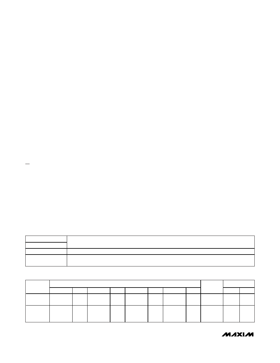
Table 1. Mode Configuration
INPUT PIN
MODE
OPERATION
0
Puts the device in mode 0. The direct-control inputs DA_ and DB_ control the switches.
1
Puts the device in mode 1. The switches are controlled by the I2C interface. DO_ becomes an active output.
Inputs DB1 and DB2 are high impedance.
Table 2. I2C Register Map
BIT
POWER-UP
REGISTER
7
6
5
432
1
0
ADDRESS
BINARY
HEX
R0
BBEN
BBSE
L1
BBSEL0
BAEN
BASEL1
BASE
L0
X
0x00
0000
00
R1
DO3
High
Impedance
DO3
Data
DO2
High
Impedance
DO2
Data
DO1
High
Impedance
DO1
Data
DO0
High
Impedance
DO0
Data
0x01
1010
AA
相关PDF资料 |
PDF描述 |
|---|---|
| DSPIC30F5015T-30I/PT | IC DSPIC MCU/DSP 66K 64TQFP |
| MAX355EPE+ | IC MULTIPLEXER DUAL 4X1 16DIP |
| DSPIC33FJ64MC510A-E/PF | IC DSPIC MCU/DSP 64K 100-TQFP |
| PIC16C72-10I/SS | IC MCU OTP 2KX14 A/D PWM 28SSOP |
| GRM3195C2A512JA01D | CAP CER 5100PF 100V 5% NP0 1206 |
相关代理商/技术参数 |
参数描述 |
|---|---|
| MAX4814EECB+ | 功能描述:多路器开关 IC DVI/HDMI 2:4 Low-f Fanout Switch RoHS:否 制造商:Texas Instruments 通道数量:1 开关数量:4 开启电阻(最大值):7 Ohms 开启时间(最大值): 关闭时间(最大值): 传播延迟时间:0.25 ns 工作电源电压:2.3 V to 3.6 V 工作电源电流: 最大工作温度:+ 85 C 安装风格:SMD/SMT 封装 / 箱体:UQFN-16 |
| MAX4814EECB+T | 功能描述:多路器开关 IC DVI/HDMI 2:4 Low-f Fanout Switch RoHS:否 制造商:Texas Instruments 通道数量:1 开关数量:4 开启电阻(最大值):7 Ohms 开启时间(最大值): 关闭时间(最大值): 传播延迟时间:0.25 ns 工作电源电压:2.3 V to 3.6 V 工作电源电流: 最大工作温度:+ 85 C 安装风格:SMD/SMT 封装 / 箱体:UQFN-16 |
| MAX4815ETE | 功能描述:模拟开关 IC RoHS:否 制造商:Texas Instruments 开关数量:2 开关配置:SPDT 开启电阻(最大值):0.1 Ohms 切换电压(最大): 开启时间(最大值): 关闭时间(最大值): 工作电源电压:2.7 V to 4.5 V 最大工作温度:+ 85 C 安装风格:SMD/SMT 封装 / 箱体:DSBGA-16 |
| MAX4815ETE+ | 功能描述:模拟开关 IC T1/E1 SPST Analog Switch RoHS:否 制造商:Texas Instruments 开关数量:2 开关配置:SPDT 开启电阻(最大值):0.1 Ohms 切换电压(最大): 开启时间(最大值): 关闭时间(最大值): 工作电源电压:2.7 V to 4.5 V 最大工作温度:+ 85 C 安装风格:SMD/SMT 封装 / 箱体:DSBGA-16 |
| MAX4815ETE+T | 功能描述:模拟开关 IC T1/E1 SPST Analog Switch RoHS:否 制造商:Texas Instruments 开关数量:2 开关配置:SPDT 开启电阻(最大值):0.1 Ohms 切换电压(最大): 开启时间(最大值): 关闭时间(最大值): 工作电源电压:2.7 V to 4.5 V 最大工作温度:+ 85 C 安装风格:SMD/SMT 封装 / 箱体:DSBGA-16 |
发布紧急采购,3分钟左右您将得到回复。