- 您现在的位置:买卖IC网 > PDF目录10618 > MAX4895EETE+ (Maxim Integrated Products)IC PORT PROTECTOR VGA 16TQFN PDF资料下载
参数资料
| 型号: | MAX4895EETE+ |
| 厂商: | Maxim Integrated Products |
| 文件页数: | 2/8页 |
| 文件大小: | 0K |
| 描述: | IC PORT PROTECTOR VGA 16TQFN |
| 产品培训模块: | Lead (SnPb) Finish for COTS Obsolescence Mitigation Program |
| 标准包装: | 100 |
| 类型: | VGA 端口保护器 |
| 应用: | 台式,笔记本电脑 |
| 安装类型: | 表面贴装 |
| 封装/外壳: | 16-WFQFN 裸露焊盘 |
| 供应商设备封装: | 16-TQFN-EP(3x3) |
| 包装: | 管件 |
MAX4895E
VGA Port Protector
2
_______________________________________________________________________________________
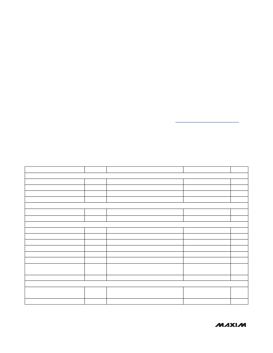
ABSOLUTE MAXIMUM RATINGS
ELECTRICAL CHARACTERISTICS
(VCC = +4.5V to +5.5V, VL = +2.0V to VCC, TA = TMIN to TMAX, unless otherwise noted. Typical values are at VCC = +5.0V,
VL = +3.3V, and TA = +25°C.) (Note 2)
Stresses beyond those listed under “Absolute Maximum Ratings” may cause permanent damage to the device. These are stress ratings only, and functional
operation of the device at these or any other conditions beyond those indicated in the operational sections of the specifications is not implied. Exposure to
absolute maximum rating conditions for extended periods may affect device reliability.
Note 1: Package thermal resistances were obtained using the method described in JEDEC specification JESD51-7, using a four-
layer board. For detailed information on package thermal considerations, refer to www.maxim-ic.com/thermal-tutorial.
(All voltages referenced to GND.)
VCC ........................................................................-0.3V to +6.0V
VL .............................................................-0.3V to +(VCC + 0.3V)
R, G, B, H1, V1, SCL1, SDA1...................-0.3V to +(VCC + 0.3V)
EN, H0, V0, SCL0, SDA0 ............................-0.3V to +(VL + 0.3V)
Continuous Current through SDA_, SCL_.........................±30mA
Continuous Short-Circuit Current H1, V1..........................±20mA
Continuous Power Dissipation (TA = +70°C) for multilayer board:
16-Pin TQFN (derate 20.8mW/°C above +70°C) .......1667mW
Junction-to-Case Thermal Resistance (
θJC) (Note 1) ......7°C/W
Junction-to-Ambient Thermal Resistance (
θJA)
(Note 1) ........................................................................48°C/W
Operating Temperature Range ...........................-40°C to +85°C
Junction Temperature ......................................................+150°C
Storage Temperature Range .............................-65°C to +150°C
Lead Temperature (soldering, 10s) .................................+300°C
Soldering Temperature (reflow) .......................................+260°C
PARAMETER
SYMBOL
CONDITIONS
MIN
TYP
MAX
UNITS
SUPPLY OPERATION
Supply Voltage
VCC
4.5
5.5
V
Logic Supply Voltage
VL
VCC
2
3.3
5.5
V
VCC Supply Current
ICC
VH0, VV0 = 0V, VEN = VL
0.5
5.0
μA
VL Supply Current
IL
VH0, VV0 = 0V, VEN = VL (no load)
0.5
5.0
μA
RGB CHANNELS
R, G, B Capacitance
COUT
f = 1MHz, VR,G,B = 1VP-P (Note 3)
2.2
pF
R, G, B Leakage
VCC = +5.5V
-1
+1
μA
H_, V_, EN CHANNELS
Input Threshold Low
VIL
VL = +3.0V
0.8
V
Input Threshold High
VIH
VL = +3.6V
2.0
V
Input Hysteresis
VHYST
100
mV
Input Leakage Current
ILEAK
VL = +3.3V, VCC = +5.5V
-1
+1
μA
Output-Voltage Low
VOL
IOUT = 10mA sink, VCC = +4.5V
0.8
V
Output-Voltage High
VOH
IOUT = 10mA source, VCC = +4.5V
2.4
V
Propagation Delay
tPD
RL = 2.2k , CL = 10pF, VOL = +0.8V,
VOH = +2.4V
15
ns
Enable Time
tON, tOFF
15
ns
SDA_, SCL_ (DDC) CHANNELS
On-Resistance, SDA, SCL
RON
VCC = +5.5V, ISDA, SCL = ±10mA,
VSDA, SCL = +0.5V
20
55
Leakage Current, SDA, SCL
ILEAK
VL = 0V
-1
+1
μA
相关PDF资料 |
PDF描述 |
|---|---|
| VE-JW4-MW-F3 | CONVERTER MOD DC/DC 48V 100W |
| VE-JW4-MW-F2 | CONVERTER MOD DC/DC 48V 100W |
| VE-JW4-MW-F1 | CONVERTER MOD DC/DC 48V 100W |
| MAX222EWN+ | IC 2DVR/2RCVR RS232 5V 18-SOIC |
| MAX222EWN | IC 2DVR/2RCVR RS232 5V 18-SOIC |
相关代理商/技术参数 |
参数描述 |
|---|---|
| MAX4895EETE+ | 功能描述:视频 IC VGA Port Protector RoHS:否 制造商:Fairchild Semiconductor 工作电源电压:5 V 电源电流:80 mA 最大工作温度:+ 85 C 封装 / 箱体:TSSOP-28 封装:Reel |
| MAX4895EETE+T | 功能描述:视频 IC VGA Port Protector RoHS:否 制造商:Fairchild Semiconductor 工作电源电压:5 V 电源电流:80 mA 最大工作温度:+ 85 C 封装 / 箱体:TSSOP-28 封装:Reel |
| MAX4895EETE-T | 功能描述:视频 IC RoHS:否 制造商:Fairchild Semiconductor 工作电源电压:5 V 电源电流:80 mA 最大工作温度:+ 85 C 封装 / 箱体:TSSOP-28 封装:Reel |
| MAX4896ATP+ | 功能描述:功率驱动器IC 8Ch Relay/Load Driver RoHS:否 制造商:Micrel 产品:MOSFET Gate Drivers 类型:Low Cost High or Low Side MOSFET Driver 上升时间: 下降时间: 电源电压-最大:30 V 电源电压-最小:2.75 V 电源电流: 最大功率耗散: 最大工作温度:+ 85 C 安装风格:SMD/SMT 封装 / 箱体:SOIC-8 封装:Tube |
| MAX4896ATP+T | 功能描述:功率驱动器IC 8Ch Relay/Load Driver RoHS:否 制造商:Micrel 产品:MOSFET Gate Drivers 类型:Low Cost High or Low Side MOSFET Driver 上升时间: 下降时间: 电源电压-最大:30 V 电源电压-最小:2.75 V 电源电流: 最大功率耗散: 最大工作温度:+ 85 C 安装风格:SMD/SMT 封装 / 箱体:SOIC-8 封装:Tube |
发布紧急采购,3分钟左右您将得到回复。