- 您现在的位置:买卖IC网 > PDF目录11038 > MAX4948EBA+T (Maxim Integrated Products)IC SWITCH HEX SPDT 25UCSP PDF资料下载
参数资料
| 型号: | MAX4948EBA+T |
| 厂商: | Maxim Integrated Products |
| 文件页数: | 6/13页 |
| 文件大小: | 0K |
| 描述: | IC SWITCH HEX SPDT 25UCSP |
| 标准包装: | 2,500 |
| 功能: | 开关 |
| 电路: | 6 x SPDT |
| 导通状态电阻: | 5.5 欧姆 |
| 电压电源: | 单电源 |
| 电压 - 电源,单路/双路(±): | 1.8 V ~ 5.5 V |
| 电流 - 电源: | 10µA |
| 工作温度: | -40°C ~ 85°C |
| 安装类型: | 表面贴装 |
| 封装/外壳: | 25-WFBGA,CSPBGA |
| 供应商设备封装: | 25-UCSP(5x5) |
| 包装: | 带卷 (TR) |
MAX4947/MAX4948
Hex SPDT Data Switch
2
_______________________________________________________________________________________
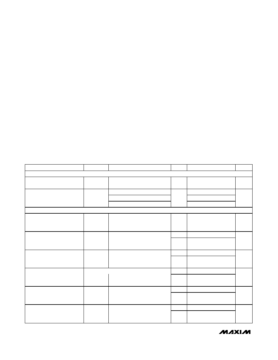
ABSOLUTE MAXIMUM RATINGS
ELECTRICAL CHARACTERISTICS
(VCC = +2.7V to +5.5V, TA = -40°C to +85°C, unless otherwise noted. Typical values are at VCC = +3V, TA = +25°C.) (Notes 2, 3)
Stresses beyond those listed under “Absolute Maximum Ratings” may cause permanent damage to the device. These are stress ratings only, and functional
operation of the device at these or any other conditions beyond those indicated in the operational sections of the specifications is not implied. Exposure to
absolute maximum rating conditions for extended periods may affect device reliability.
VCC to GND ...........................................................-0.3V to +6.0V
All other pins to GND (Note 1) ......................-0.3V to VCC + 0.3V
Continuous Current
NO_, NC_, COM_ .......................................................±100mA
Peak Current NO_, NC_, COM_
(pulsed at 1ms, 50% Duty Cycle)................................±200mA
(pulsed at 1ms, 10% Duty Cycle)................................±300mA
Continuous Power Dissipation (TA = +70°C)
25-Bump UCSP (derate 12.2mW/°C above +70°C) ....976mW
24-Pin TQFN (derate 20.8mW/°C above +70°C) .......1667mW
Operating Temperature Range ...........................-40°C to +85°C
Junction Temperature ........................................................150°C
Storage Temperature Range .............................-65°C to +150°C
Bump Temperature (soldering)
Infrared (15s) ...............................................................+220°C
Vapor Phase (60s) ...........................................................+215°C
Lead Temperature (soldering) .........................................+300°C
PARAMETER
SYMBOL
CONDITIONS
TA
MIN
TYP
MAX
UNITS
POWER SUPPLY
Power-Supply Range
VCC
TMIN to
TMAX
1.8
5.5
V
VCC = 5.5V, VCB_ = 0V or VCC
1.0
VCC = 2.7V, VCB_ = 1.6V or 0.5V
5
Power-Supply Current
ICC
VCC = 5.5V, VCB_ = 1.6V or 0.5V
TMIN to
TMAX
10
A
ANALOG SWITCH
Analog Signal Range
VNO_, VNC_,
VCOM_,
TMIN to
TMAX
0VCC
V
+25°C
4.0
5.5
On-Resistance (Note 4)
RON
VCC = 2.7V, ICOM_ = 10mA;
VNC_ or VNO_ = 0 or VCC
TMIN to
TMAX
6.5
Ω
+25°C
0.3
0.5
On-Resistance Match Between
Channels (Notes 4, 5)
ΔRON
VCC = 2.7V, ICOM_ = 10mA;
VNO_ or VNC_ = 0 or VCC
TMIN to
TMAX
0.6
Ω
+25°C
0.5
1
On-Resistance Flatness
(Notes 4, 6)
RFLAT
VCC = 2.7V, ICOM_ = 10mA;
VNC_ or VNO_ = 0 or VCC
TMIN to
TMAX
1.2
Ω
+25°C
-3
+3
NO_ or NC_ Off-Leakage
Current
INO_(OFF) or
INC_(OFF)
VCC = 3.6V; VCOM_ = 3.6V, 0;
VNO_ or VNC_ = 0, 3.6V
TMIN to
TMAX
-10
+10
nA
+25°C
-6
+6
COM_ On-Leakage Current
INO_(ON)
VCC = 3.6V; VCOM_ = 3.6V, 0;
VNO_ or VNC_ = 3.6V, 0 or
unconnected
TMIN to
TMAX
-10
+10
nA
Note 1: Signals on CB_, NO_, NC_, COM_,
EN exceeding VCC or GND are clamped by internal diodes. Limit forward-diode current
to maximum current rating.
相关PDF资料 |
PDF描述 |
|---|---|
| VI-B4F-IY-F2 | CONVERTER MOD DC/DC 72V 50W |
| MAX4828ELT+T | IC SWITCH 1X1 6UTDFN |
| VI-B4D-IY-F4 | CONVERTER MOD DC/DC 85V 50W |
| MAX4816ETE+T | IC SWITCH QUAD SPST 16TQFN |
| VI-B4D-IY-F3 | CONVERTER MOD DC/DC 85V 50W |
相关代理商/技术参数 |
参数描述 |
|---|---|
| MAX4948ERA+ | 制造商:Maxim Integrated Products 功能描述:HEX SPDT DATA SWITCH - Rail/Tube |
| MAX4948ERA+T | 制造商:Maxim Integrated Products 功能描述:HEX SPDT DATA SWITCH - Tape and Reel |
| MAX4948ETG+ | 功能描述:模拟开关 IC Hex SPDT Data Switch RoHS:否 制造商:Texas Instruments 开关数量:2 开关配置:SPDT 开启电阻(最大值):0.1 Ohms 切换电压(最大): 开启时间(最大值): 关闭时间(最大值): 工作电源电压:2.7 V to 4.5 V 最大工作温度:+ 85 C 安装风格:SMD/SMT 封装 / 箱体:DSBGA-16 |
| MAX4948ETG+T | 功能描述:模拟开关 IC Hex SPDT Data Switch RoHS:否 制造商:Texas Instruments 开关数量:2 开关配置:SPDT 开启电阻(最大值):0.1 Ohms 切换电压(最大): 开启时间(最大值): 关闭时间(最大值): 工作电源电压:2.7 V to 4.5 V 最大工作温度:+ 85 C 安装风格:SMD/SMT 封装 / 箱体:DSBGA-16 |
| MAX4948EVKIT+ | 功能描述:交换机 IC 开发工具 MAX4948 Eval Kit RoHS:否 制造商:Maxim Integrated 产品:Evaluation Kits 类型:USB Power Switches 工具用于评估:MAX4984E 工作电源电压:2.8 V to 5.5 V |
发布紧急采购,3分钟左右您将得到回复。