- 您现在的位置:买卖IC网 > PDF目录5506 > MAX494ESD+T (Maxim Integrated Products)IC OPAMP QD MICROPWR R/R 14SOIC PDF资料下载
参数资料
| 型号: | MAX494ESD+T |
| 厂商: | Maxim Integrated Products |
| 文件页数: | 4/17页 |
| 文件大小: | 0K |
| 描述: | IC OPAMP QD MICROPWR R/R 14SOIC |
| 产品培训模块: | Lead (SnPb) Finish for COTS Obsolescence Mitigation Program |
| 标准包装: | 2,500 |
| 放大器类型: | 通用 |
| 电路数: | 4 |
| 输出类型: | 满摆幅 |
| 转换速率: | 0.2 V/µs |
| 增益带宽积: | 500kHz |
| 电流 - 输入偏压: | 25nA |
| 电压 - 输入偏移: | 200µV |
| 电流 - 电源: | 150µA |
| 电流 - 输出 / 通道: | 30mA |
| 电压 - 电源,单路/双路(±): | 2.7 V ~ 6 V,±1.35 V ~ 3 V |
| 工作温度: | -40°C ~ 85°C |
| 安装类型: | 表面贴装 |
| 封装/外壳: | 14-SOIC(0.154",3.90mm 宽) |
| 供应商设备封装: | 14-SOIC |
| 包装: | 带卷 (TR) |
MAX492/MAX494/MAX495
Single/Dual/Quad, Micropower,
Single-Supply Rail-to-Rail Op Amps
the op amp in an inverting configuration (Figure 3a);
connect resistor R3 between the noninverting input and
the input signal when using the op amp in a noninvert-
ing configuration (Figure 3b). Select R3 to equal the
parallel combination of R1 and R2. High source resis-
tances will degrade noise performance, due to the ther-
mal noise of the resistor and the input current noise
(which is multiplied by the source resistance).
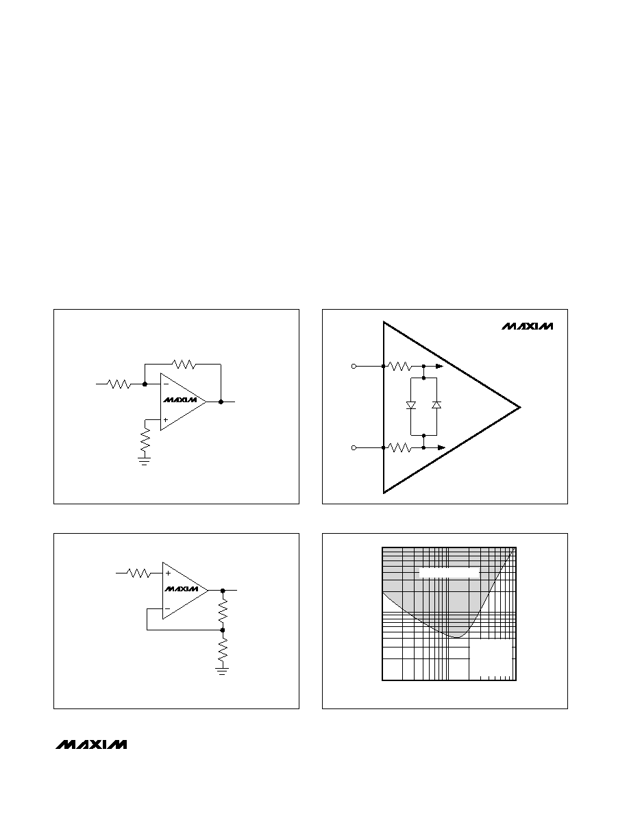
Input Stage Protection Circuitry
The MAX492/MAX494/MAX495 include internal protec-
tion circuitry that prevents damage to the precision
input stage from large differential input voltages. This
protection circuitry consists of back-to-back diodes
between IN+ and IN- with two 1.7k
resistors in series
(Figure 4). The diodes limit the differential voltage
applied to the amplifiers’ internal circuitry to no more
than VF, where VF is the diodes’ forward-voltage drop
(about 0.7V at +25°C).
Input bias current for the ICs (±25nA typical) is speci-
fied for the small differential input voltages. For large
differential input voltages (exceeding VF), this protec-
tion circuitry increases the input current at IN+ and IN-:
(VIN+ - VIN- ) - VF
Input Current = ———————————
2 x 1.7k
For comparator applications requiring large differential
voltages (greater than VF), you can limit the input cur-
rent that flows through the diodes with external resistors
R1
VOUT
R3 = R2 II R1
R3
VIN
R2
MAX49_
Figure 3a. Reducing Offset Error Due to Bias Current:
Inverting Configuration
R3
VOUT
R3 = R2 II R1
VIN
R1
R2
MAX49_
MAX492
MAX494
MAX495
1.7k
1.7k
TO INTERNAL
CIRCUITRY
TO INTERNAL
CIRCUITRY
IN–
IN+
Figure 4. Input Stage Protection Circuitry
10,000
100
1
10
100
MAX492-FG
04
RESISTIVE LOAD (k
)
CAPACITIVE
LOAD
(pF)
1000
UNSTABLE REGION
VCC = +5V
VOUT = VCC/2
RL TO VEE
AV = +1
Figure 5. Capacitive-Load Stable Region Sourcing Current
______________________________________________________________________________________
11
Figure 3b. Reducing Offset Error Due to Bias Current:
Noninverting Configuration
相关PDF资料 |
PDF描述 |
|---|---|
| BK/AGC-V-9-R | FUSE 9A 250V FAST GLASS AXIAL |
| BK/AGC-V-8-R | FUSE 8A 250V FAST GLASS AXIAL |
| BK/AGC-V-30-R | FUSE 30A 32V FAST GLASS AXIAL |
| 34810 | CONN RING 14-16HD AWG #5/16 PIDG |
| MAX409ACPA+ | IC OPAMP GP R-R 150KHZ 8PDIP |
相关代理商/技术参数 |
参数描述 |
|---|---|
| MAX494MJD | 功能描述:运算放大器 - 运放 RoHS:否 制造商:STMicroelectronics 通道数量:4 共模抑制比(最小值):63 dB 输入补偿电压:1 mV 输入偏流(最大值):10 pA 工作电源电压:2.7 V to 5.5 V 安装风格:SMD/SMT 封装 / 箱体:QFN-16 转换速度:0.89 V/us 关闭:No 输出电流:55 mA 最大工作温度:+ 125 C 封装:Reel |
| MAX4950ACTX+ | 功能描述:均衡器 Single PCIe Re-Driver RoHS:否 制造商:Texas Instruments |
| MAX4950ACTX+T | 功能描述:IC PCIE REDRIVER DUAL 36-TQFN RoHS:是 类别:集成电路 (IC) >> 接口 - 驱动器,接收器,收发器 系列:- 标准包装:1,240 系列:GD 类型:收发器 驱动器/接收器数:3/5 规程:RS232 电源电压:4.5 V ~ 5.5 V 安装类型:通孔 封装/外壳:20-DIP(0.300",7.62mm) 供应商设备封装:20-PDIP 包装:管件 |
| MAX4950CTO+ | 功能描述:IC PCIE REDRIVER 3.3V 42TQFN RoHS:是 类别:集成电路 (IC) >> 接口 - 驱动器,接收器,收发器 系列:- 标准包装:2,500 系列:- 类型:驱动器 驱动器/接收器数:4/0 规程:RS422 电源电压:4.5 V ~ 5.5 V 安装类型:表面贴装 封装/外壳:16-SOIC(0.154",3.90mm 宽) 供应商设备封装:16-SOIC N 包装:带卷 (TR) |
| MAX4950CTO+T | 功能描述:IC PCIE REDRIVER 3.3V 42TQFN RoHS:是 类别:集成电路 (IC) >> 接口 - 驱动器,接收器,收发器 系列:- 标准包装:1,240 系列:GD 类型:收发器 驱动器/接收器数:3/5 规程:RS232 电源电压:4.5 V ~ 5.5 V 安装类型:通孔 封装/外壳:20-DIP(0.300",7.62mm) 供应商设备封装:20-PDIP 包装:管件 |
发布紧急采购,3分钟左右您将得到回复。