- 您现在的位置:买卖IC网 > PDF目录4574 > MAX4959EUB+T (Maxim Integrated Products)IC CTLR HI VOLTAGE OVP 10-MSOP PDF资料下载
参数资料
| 型号: | MAX4959EUB+T |
| 厂商: | Maxim Integrated Products |
| 文件页数: | 13/17页 |
| 文件大小: | 0K |
| 描述: | IC CTLR HI VOLTAGE OVP 10-MSOP |
| 产品培训模块: | Lead (SnPb) Finish for COTS Obsolescence Mitigation Program |
| 标准包装: | 2,500 |
| 类型: | 过压保护控制器 |
| 应用: | PC,PDA |
| 安装类型: | 表面贴装 |
| 封装/外壳: | 10-TFSOP,10-MSOP(0.118",3.00mm 宽) |
| 供应商设备封装: | 10-µMAX |
| 包装: | 带卷 (TR) |
Detailed Description
The MAX4959/MAX4960 provide up to +28V overvoltage
protection for low-voltage systems. When the input volt-
age exceeds the overvoltage trip level, the MAX4959/
MAX4960 turn off an external pFET to prevent damage
to the protected components.
The MAX4959/MAX4960 feature a control bit (CB) pin
that controls an external battery-switchover function that
switches in the battery when the adapter is unconnect-
ed. The host system detects when the battery switchover
must take place and pulls CB high to turn on P2. The
load current is not interrupted during battery switchover
as the body diode of P2 conducts until the CB line is dri-
ven high (see the
MAX4959 Typical Operating Circuit 1,
Figure 4).
An additional safety feature latches off pFET P1 when a
low-power adapter is plugged in. This protects the sys-
tem from seeing repeated adapter insertions and
removals when an incorrect low-power adapter is
plugged in that cannot provide sufficient current.
Undervoltage Lockout (UVLO)
The MAX4959/MAX4960 have an adjustable undervolt-
age lockout threshold ranging from +5V to +28V. When
VIN is less than the VUVLO, the device waits for a blank-
ing time, tBLANK, to see if the fault still exists. If the fault
does not exist at the end of tBLANK, P1 remains on. If
VIN is less than VUVLO for longer than the blanking
time, the device turns P1 off and P1 does not turn on
again until VIN < 0.75V. See Figure 1.
Overvoltage Lockout (OVLO)
The MAX4959/MAX4960 have an adjustable overvolt-
age lockout threshold ranging from +6V to +28V. When
VIN is greater than the VOVLO, the device turns P1 off
immediately. When VIN drops below VOVLO, P1 turns on
again after the debounce time has elapsed.
Device Operation
High-Voltage Adapter (VIN > VOVLO)
If an adapter with a voltage higher than VOVLO is
plugged in, the MAX4959/MAX4960 is in an OVP condi-
tion, so P1 is kept off or immediately turned off. There is
MAX4959/MAX4960
High-Voltage OVP with Battery Switchover
_______________________________________________________________________________________
5
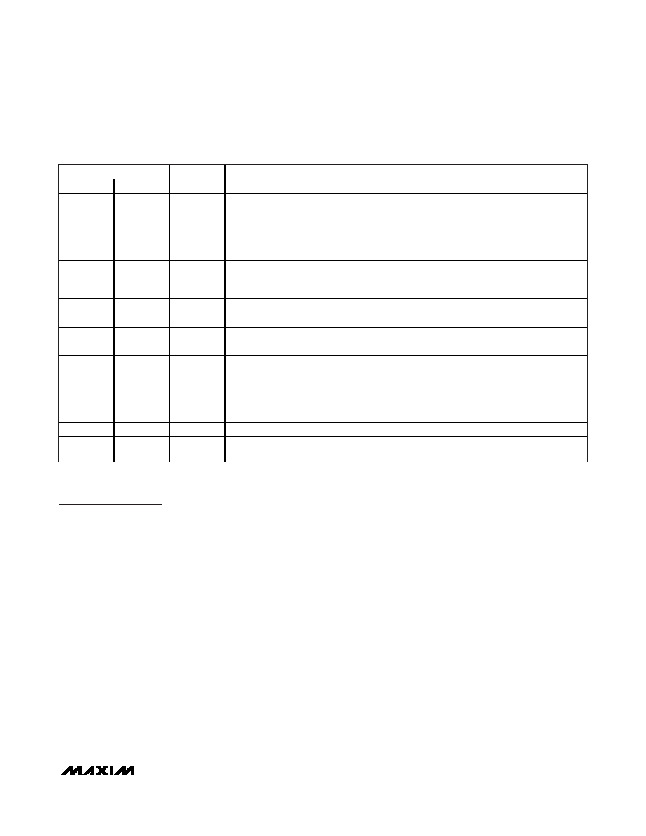
Pin Description
PIN
MAX4959
MAX4960
NAME
FUNCTION
1
GATE1
pFET Gate Drive Output Open Drain. GATE1 is actively driven low, except during fault
(OVP or UVP) condition (the external pFET is turned off). When VUVLO < VIN < VOVLO,
GATE1 is driven low (the external pFET P1 is turned on).
2, 9
9
N.C.
No Connection. Not internally connected. (Connect to ground or leave unconnected.)
—2
SOURCE1
pFET Source Output. An internal resistor is connected between SOURCE1 and GATE1.
33
IN
Voltage Input. IN is both the power-supply input and the overvoltage/undervoltage
sense input. Bypass IN to GND with a 1F ceramic capacitor to get a ±15kV protected
input. A minimum 0.1F ceramic capacitor is required for proper operation.
4
UVS
Undervoltage Threshold Set Input. Connect UVS to an external resistive divider from IN to
GND to set the undervoltage lockout threshold. (See Typical Operating Circuits.)
5
OVS
Overvoltage Threshold Set Input. Connect OVS to an external resistive divider from
IN to GND to set the overvoltage lockout threshold. (See Typical Operating Circuits.)
66
VDD
Internal Power-Supply Output. Bypass VDD to GND with a 0.1F minimum capacitor.
VDD powers the internal power-on reset circuits. (See the VDD Capacitor Selection section.)
77
CB
Battery Switchover Control Input. When CB is high, GATE1 is high (P1 is off), and GATE2
is low (P2 is on). When CB is low, GATE1 is controlled by internal logic and GATE2 is
high (P2 is off). GATE1 is controlled by CB only if VUVLO < VIN < VOVLO.
8
GND
Ground
10
GATE2
pFET Gate Drive Output, Open Drain. When CB is high, GATE2 is low (P2 is on).
When CB is low, GATE2 is high impedance (P2 is off).
相关PDF资料 |
PDF描述 |
|---|---|
| MAX4960ELB+T | IC CTLR HI VOLTAGE OVP 10-UDFN |
| MAX4944BELA+T | IC CTLR OVP W/FET 6.35V 8-UDFN |
| MAX4945BELA+T | IC CTLR OVP W/FET 5.80V 8-UDFN |
| LFXP20E-3FN256C | IC FPGA 19.7KLUTS 188I/O 256-BGA |
| LFXP20C-3FN256C | IC FPGA 19.7KLUTS 188I/O 256-BGA |
相关代理商/技术参数 |
参数描述 |
|---|---|
| MAX495C/D | 功能描述:运算放大器 - 运放 Single Micropower Single-Supply Rail-to-Rail Op Amp RoHS:否 制造商:STMicroelectronics 通道数量:4 共模抑制比(最小值):63 dB 输入补偿电压:1 mV 输入偏流(最大值):10 pA 工作电源电压:2.7 V to 5.5 V 安装风格:SMD/SMT 封装 / 箱体:QFN-16 转换速度:0.89 V/us 关闭:No 输出电流:55 mA 最大工作温度:+ 125 C 封装:Reel |
| MAX495C/D DIE | 制造商:Maxim Integrated Products 功能描述: |
| MAX495CPA | 功能描述:运算放大器 - 运放 Single uPower Single Supply Rail-Rail RoHS:否 制造商:STMicroelectronics 通道数量:4 共模抑制比(最小值):63 dB 输入补偿电压:1 mV 输入偏流(最大值):10 pA 工作电源电压:2.7 V to 5.5 V 安装风格:SMD/SMT 封装 / 箱体:QFN-16 转换速度:0.89 V/us 关闭:No 输出电流:55 mA 最大工作温度:+ 125 C 封装:Reel |
| MAX495CPA+ | 功能描述:运算放大器 - 运放 Single uPower Single Supply Rail-Rail RoHS:否 制造商:STMicroelectronics 通道数量:4 共模抑制比(最小值):63 dB 输入补偿电压:1 mV 输入偏流(最大值):10 pA 工作电源电压:2.7 V to 5.5 V 安装风格:SMD/SMT 封装 / 箱体:QFN-16 转换速度:0.89 V/us 关闭:No 输出电流:55 mA 最大工作温度:+ 125 C 封装:Reel |
| MAX495CSA | 功能描述:运算放大器 - 运放 Single uPower Single Supply Rail-Rail RoHS:否 制造商:STMicroelectronics 通道数量:4 共模抑制比(最小值):63 dB 输入补偿电压:1 mV 输入偏流(最大值):10 pA 工作电源电压:2.7 V to 5.5 V 安装风格:SMD/SMT 封装 / 箱体:QFN-16 转换速度:0.89 V/us 关闭:No 输出电流:55 mA 最大工作温度:+ 125 C 封装:Reel |
发布紧急采购,3分钟左右您将得到回复。