- 您现在的位置:买卖IC网 > PDF目录1944 > MAX4969CTO+T (Maxim Integrated Products)IC MUX/REDRIVER PCIE 42TQFN PDF资料下载
参数资料
| 型号: | MAX4969CTO+T |
| 厂商: | Maxim Integrated Products |
| 文件页数: | 2/10页 |
| 文件大小: | 0K |
| 描述: | IC MUX/REDRIVER PCIE 42TQFN |
| 产品培训模块: | Lead (SnPb) Finish for COTS Obsolescence Mitigation Program |
| 标准包装: | 2,500 |
| 类型: | 转接驱动器 |
| 驱动器/接收器数: | 1/1 |
| 规程: | PCIe? |
| 电源电压: | 3 V ~ 3.6 V |
| 安装类型: | 表面贴装 |
| 封装/外壳: | 42-WFQFN 裸露焊盘 |
| 供应商设备封装: | 42-TQFN-EP(3.5x9) |
| 包装: | 带卷 (TR) |
PCIe, Single Lane, 2:1/1:2 Multiplexer and
Redriver with Equalization
MAX4969
Maxim cannot assume responsibility for use of any circuitry other than circuitry entirely embodied in a Maxim product. No circuit patent licenses are implied.
Maxim reserves the right to change the circuitry and specifications without notice at any time.
10
Maxim Integrated Products, 120 San Gabriel Drive, Sunnyvale, CA 94086 408-737-7600
2009 Maxim Integrated Products
Maxim is a registered trademark of Maxim Integrated Products, Inc.
Applications Information
Layout
Circuit board layout and design can significantly affect
the performance of the MAX4969. Use good high-fre-
quency design techniques, including minimizing ground
inductance and using controlled-impedance transmis-
sion lines on data signals. It is recommended to run
receive and transmit on different layers to minimize
crosstalk and to place 1FF and 0.01FF power-supply
bypass capacitors in parallel as close to VCC as possible
on each VCC pin. Always connect VCC to a power plane.
Exposed Pad Package
The exposed-pad, 42-pin TQFN package incorporates
features that provide a very low thermal resistance path
for heat removal from the IC. The exposed pad on the
MAX4969 must be soldered to the circuit board ground
plane for proper thermal performance. For more informa-
tion on exposed-pad packages, refer to Application Note
862: HFAN-08.1: Thermal Considerations of QFN and
Other Exposed-Paddle Packages.
Power-Supply Sequencing
Caution: Do not exceed the absolute maximum rat-
ings because stresses beyond the listed ratings may
cause permanent damage to the device.
Proper power-supply sequencing is recommended for
all devices. Always apply GND then VCC before apply-
ing signals, especially if the signal is not current limited.
Chip Information
PROCESS: BiCMOS
Package Information
For the latest package outline information and land pat-
terns, go to www.maxim-ic.com/packages. Note that
a “+”, “#”, or “-” in the package code indicates RoHS
status only. Package drawings may show a different suf-
fix character, but the drawing pertains to the package
regardless of RoHS status.
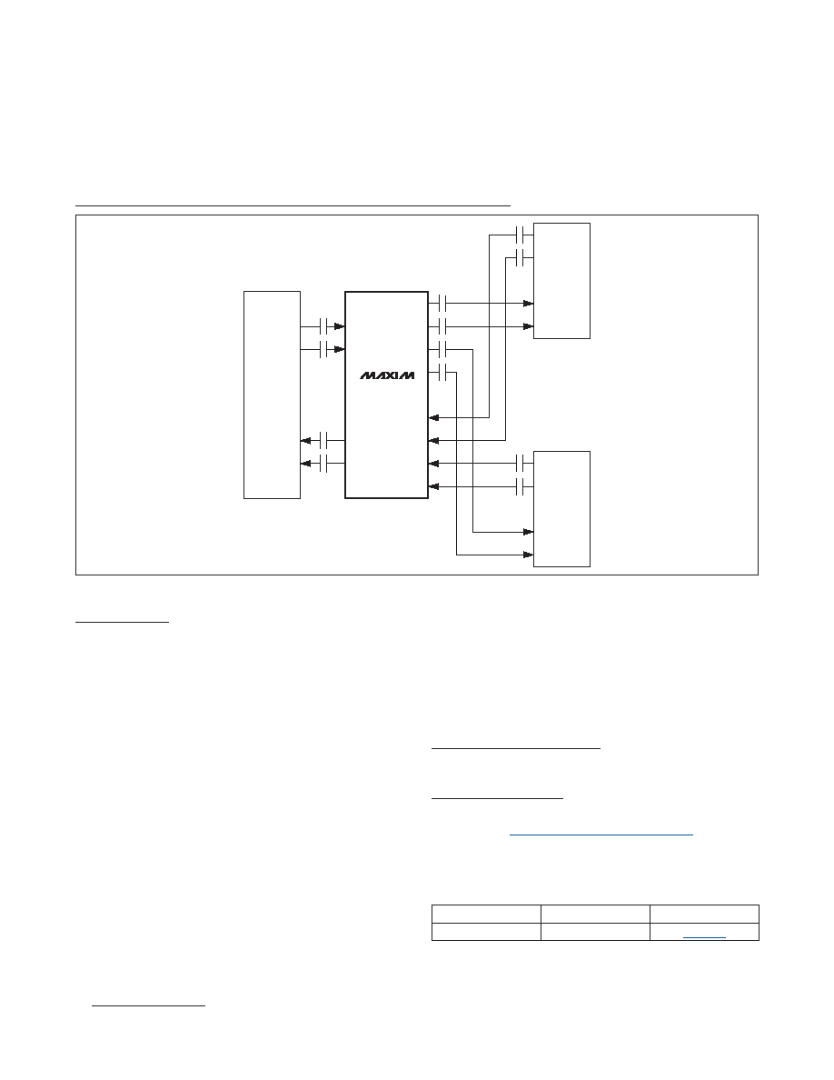
Typical Application Circuit
MAX4969
IN
OUT
Tx
OUTA
OUTB
INA
INB
Rx
PCIe
HOST
Rx
Tx
PCIe
DEVICE B
Rx
Tx
PCIe
DEVICE A
PACKAGE TYPE
PACKAGE CODE
DOCUMENT NO.
42 TQFN-EP
T423590+1
相关PDF资料 |
PDF描述 |
|---|---|
| MAX4984EEVB+ | IC USB SWITCH DPDT 10UTQFN |
| MAX4986ETO+T | IC MUX/DEMUX SAS/SATA 42TQFN |
| MAX4987AEETA+T | IC CTLR OVP USB ESD PROT 8TDFN |
| MAX4989ETD+T | IC CROSSPOINT SWITCH 14TDFN |
| MAX4993EVB+ | IC SWITCH DPDT 10UTQFN |
相关代理商/技术参数 |
参数描述 |
|---|---|
| MAX496C/D | 功能描述:运算放大器 - 运放 RoHS:否 制造商:STMicroelectronics 通道数量:4 共模抑制比(最小值):63 dB 输入补偿电压:1 mV 输入偏流(最大值):10 pA 工作电源电压:2.7 V to 5.5 V 安装风格:SMD/SMT 封装 / 箱体:QFN-16 转换速度:0.89 V/us 关闭:No 输出电流:55 mA 最大工作温度:+ 125 C 封装:Reel |
| MAX496CPE | 功能描述:运算放大器 - 运放 RoHS:否 制造商:STMicroelectronics 通道数量:4 共模抑制比(最小值):63 dB 输入补偿电压:1 mV 输入偏流(最大值):10 pA 工作电源电压:2.7 V to 5.5 V 安装风格:SMD/SMT 封装 / 箱体:QFN-16 转换速度:0.89 V/us 关闭:No 输出电流:55 mA 最大工作温度:+ 125 C 封装:Reel |
| MAX496CPE+ | 功能描述:运算放大器 - 运放 RoHS:否 制造商:STMicroelectronics 通道数量:4 共模抑制比(最小值):63 dB 输入补偿电压:1 mV 输入偏流(最大值):10 pA 工作电源电压:2.7 V to 5.5 V 安装风格:SMD/SMT 封装 / 箱体:QFN-16 转换速度:0.89 V/us 关闭:No 输出电流:55 mA 最大工作温度:+ 125 C 封装:Reel |
| MAX496CSE | 功能描述:运算放大器 - 运放 RoHS:否 制造商:STMicroelectronics 通道数量:4 共模抑制比(最小值):63 dB 输入补偿电压:1 mV 输入偏流(最大值):10 pA 工作电源电压:2.7 V to 5.5 V 安装风格:SMD/SMT 封装 / 箱体:QFN-16 转换速度:0.89 V/us 关闭:No 输出电流:55 mA 最大工作温度:+ 125 C 封装:Reel |
| MAX496CSE+ | 功能描述:运算放大器 - 运放 RoHS:否 制造商:STMicroelectronics 通道数量:4 共模抑制比(最小值):63 dB 输入补偿电压:1 mV 输入偏流(最大值):10 pA 工作电源电压:2.7 V to 5.5 V 安装风格:SMD/SMT 封装 / 箱体:QFN-16 转换速度:0.89 V/us 关闭:No 输出电流:55 mA 最大工作温度:+ 125 C 封装:Reel |
发布紧急采购,3分钟左右您将得到回复。