- 您现在的位置:买卖IC网 > PDF目录1944 > MAX4986ETO+T (Maxim Integrated Products)IC MUX/DEMUX SAS/SATA 42TQFN PDF资料下载
参数资料
| 型号: | MAX4986ETO+T |
| 厂商: | Maxim Integrated Products |
| 文件页数: | 7/14页 |
| 文件大小: | 0K |
| 描述: | IC MUX/DEMUX SAS/SATA 42TQFN |
| 标准包装: | 2,500 |
| 功能: | 多路复用器/多路分解器 |
| 电路: | 1 x 2:1 |
| 电压电源: | 单电源 |
| 电压 - 电源,单路/双路(±): | 3.3V |
| 电流 - 电源: | 145mA |
| 工作温度: | -40°C ~ 85°C |
| 安装类型: | * |
| 封装/外壳: | * |
| 供应商设备封装: | * |
| 包装: | * |
SAS/SATA Single Lane 2:1/1:2 Multiplexer/
Demultiplexer Plus Redriver with Equalization
MAX4986
2
Stresses beyond those listed under “Absolute Maximum Ratings” may cause permanent damage to the device. These are stress ratings only, and functional
operation of the device at these or any other conditions beyond those indicated in the operational sections of the specifications is not implied. Exposure to absolute
maximum rating conditions for extended periods may affect device reliability.
(Voltages Referenced to GND.)
VCC ..................................................................... -0.3V to +4.0V
All Other Pins (Note 1) ........................... -0.3V to (VCC + 0.3V)
Continuous Current IN_P, IN_M, OUT_P, OUT_M ........ Q30mA
Peak Current IN_P, IN_M, OUT_P, OUT_M for 1Fs .... Q100mA
Continuous Power Dissipation (TA = +70NC)
42-Pin TQFN (derate 34.5mW/NC above +70NC) .... 2758mW
Operating Temperature Range ........................ -40NC to +85NC
Junction Temperature Range ........................ -40NC to +150NC
Storage Temperature Range ......................... -65NC to +150NC
Lead Temperature (soldering, 10s) ...............................+300NC
Soldering Temperature (reflow) .....................................+260NC
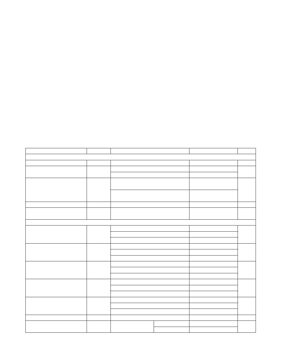
ELECTRICAL CHARACTERISTICS
(VCC = +3.0V to +3.6V, CCL = 10nF coupling capacitor on each input and output, RL = 50I on each input and output, TA = 0NC to +70NC
(MAX4986C), TA = -40NC to +85NC (MAX4986E), unless otherwise noted. Typical values are at VCC = +3.3V and TA = +25NC.) (Note 2)
ABSOLUTE MAXIMUM RATINGS
Note 1: All I/O pins are clamped by internal diodes.
PARAMETER
SYMBOL
CONDITIONS
MIN
TYP
MAX
UNITS
DC PERFORMANCE
Power-Supply Range
VCC
3.0
3.6
V
Standby Current
ISTBY
EN = 0 or EN = 1, VCC = 3.6V
2.5
4
mA
EN = 0 or EN = 1, VCC = 3.3V
1.0
2
Supply Current
ICC
OUTPE = PEA = PEB = 0,
INEQ = EQA = EQB = 0
145
170
mA
OUTPE = PEA = PEB = 1,
INEQ = EQA = EQB = 1
185
230
Input Termination, Single-Ended
RRX-SE
DC
42.5
57.5
I
Output Termination, Single-
Ended
RTX-SE
DC
42.5
57.5
I
AC PERFORMANCE
Input Return Loss, Differential
(Note 3)
SDD11
0.1GHz < f P 0.3GHz
-10
dB
0.3GHz < f P 3.0GHz
-7.9
3.0GHz < f P 6.0GHz
0
Input Return Loss,
Common Mode (Note 3)
SCC11
0.1GHz < f P 0.3GHz
-6
dB
0.3GHz < f P 3.0GHz
-5
3.0GHz < f P 6.0GHz
0
Output Return Loss, Differential
(Note 3)
SDD22
0.1GHz < f P 0.3GHz
-10
dB
0.3GHz < f P 3.0GHz
-7.9
3.0GHz < f P 6.0GHz
0
Output Return Loss,
Common Mode (Note 3)
SCC22
0.1GHz < f P 0.3GHz
-6
dB
0.3GHz < f P 3.0GHz
-5
3.0GHz < f P 6.0GHz
0
Differential Input Voltage
VIN-DIFF
SAS 1.5Gbps, 3Gbps, MODE_ = 0
275
1600
mVP-P
SAS 6Gbps, MODE_ = 0
300
1600
SATA 1.5Gbps, 3Gbps, 6Gbps, MODE_ = 1
225
1600
Input Equalization
EQ
f = 1.5GHz, INEQ = 1
4
dB
Differential Output Voltage
VOUT-DIFF
f = 0.75GHz, 1.5GHz,
PE_ = 0
OAMP_ = 0
700
1200
mVP-P
OAMP_ = 1
425
700
相关PDF资料 |
PDF描述 |
|---|---|
| MAX4987AEETA+T | IC CTLR OVP USB ESD PROT 8TDFN |
| MAX4989ETD+T | IC CROSSPOINT SWITCH 14TDFN |
| MAX4993EVB+ | IC SWITCH DPDT 10UTQFN |
| MAX4996LETG+T | IC SWITCH TRIPLE DPDT 24TQFN |
| MAX4999ETJ+T | IC MULTIPLEXER 8X1 32TQFN |
相关代理商/技术参数 |
参数描述 |
|---|---|
| MAX4986EVKIT+ | 功能描述:交换机 IC 开发工具 MAX4986 Eval Kit RoHS:否 制造商:Maxim Integrated 产品:Evaluation Kits 类型:USB Power Switches 工具用于评估:MAX4984E 工作电源电压:2.8 V to 5.5 V |
| MAX4987AEETA+ | 制造商:Maxim Integrated Products 功能描述:OVERVOLTAGE-PROTECTION CONTROLLER W - Rail/Tube |
| MAX4987AEETA+T | 功能描述:电源开关 IC - 配电 Overvoltage-Protect Controller RoHS:否 制造商:Exar 输出端数量:1 开启电阻(最大值):85 mOhms 开启时间(最大值):400 us 关闭时间(最大值):20 us 工作电源电压:3.2 V to 6.5 V 电源电流(最大值): 最大工作温度:+ 85 C 安装风格:SMD/SMT 封装 / 箱体:SOT-23-5 |
| MAX4987AETA+T | 功能描述:电源开关 IC - 配电 Overvoltage-Protect Controller RoHS:否 制造商:Exar 输出端数量:1 开启电阻(最大值):85 mOhms 开启时间(最大值):400 us 关闭时间(最大值):20 us 工作电源电压:3.2 V to 6.5 V 电源电流(最大值): 最大工作温度:+ 85 C 安装风格:SMD/SMT 封装 / 箱体:SOT-23-5 |
| MAX4989ETD+T | 功能描述:电源开关 IC - USB USB 2.0 2 of 4 Crosspoint Switch RoHS:否 制造商:Micrel 电源电压-最小:2.7 V 电源电压-最大:5.5 V 最大工作温度:+ 85 C 最小工作温度:- 40 C 封装 / 箱体:SOIC-8 封装:Tube |
发布紧急采购,3分钟左右您将得到回复。