- 您现在的位置:买卖IC网 > Datasheet目录43 > MAX4995AFAVB+ (Maxim Integrated)IC CURRENT SWITCH 10% 10UTQFN Datasheet资料下载
参数资料
| 型号: | MAX4995AFAVB+ |
| 厂商: | Maxim Integrated |
| 文件页数: | 2/13页 |
| 文件大小: | 342K |
| 描述: | IC CURRENT SWITCH 10% 10UTQFN |
| 产品培训模块: | Lead (SnPb) Finish for COTS Obsolescence Mitigation Program |
| 标准包装: | 50 |
| 功能: | 电流开关 |
| 精确度: | ±10% |
| 输入电压: | 1.7 V ~ 5.5 V |
| 电流 - 输出: | 600mA |
| 工作温度: | -40°C ~ 125°C |
| 安装类型: | 表面贴装 |
| 封装/外壳: | 10-UFQFN |
| 供应商设备封装: | 10-UTQFN(1.4x1.8) |
| 包装: | 管件 |
50mA to 600mA Programmable
Current-Limit Switches
2 _______________________________________________________________________________________
ABSOLUTE MAXIMUM RATINGS
Stresses beyond those listed under
Absolute Maximum Ratings
may cause permanent damage to the device. These are stress ratings only, and functional
operation of the device at these or any other conditions beyond those indicated in the operational sections of the specifications is not implied. Exposure to
absolute maximum rating conditions for extended periods may affect device reliability.
IN, ON, ON, FLAG, OUT, and SETI to GND.............-0.3V to +6V
Current into Any Pin (Except IN, OUT)................................20mA
OUT Short Circuit to GND.................................................800mA
Continuous Power Dissipation (T
A
= +70癈) (Note 1)
10-Pin UTQFN (derate 6.99mW/癈 above T
A
= +70癈)..559mW
6-Pin SOT23 (derate 13.4mW/癈 above T
A
= +70癈)...1072.4mW
8-Pin TDFN (derate 11.9mW/癈 above T
A
= +70癈)....953.5mW
Junction-to-Ambient Thermal Resistance (?/DIV>
JA
)
(Note 2).....................................................................143.1癈/W
Operating Temperature Range .........................-40癈 to +125癈
Storage Temperature Range.............................-65癈 to +150癈
Junction Temperature......................................................+150癈
Lead Temperature (soldering, 10s).................................+300癈
Note 1: These power limits are defined by the thermal characteristics of the package, maximum function temperature (+150?/SPAN>C), and
the JEDEC51-7 defined setup. Maximum power dissipation could be lower, limited by the thermal-shutdown protection
included in this IC.
Note 2: Package thermal resistances were obtained using the method described in JEDEC specification JESD51-7, using a four-
layer board. For detailed information on package thermal considerations, refer to www.maxim-ic.com/thermal-tutorial
.
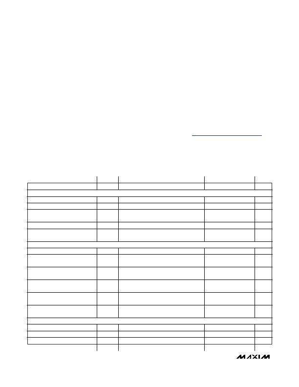
ELECTRICAL CHARACTERISTICS
(V
IN
= +1.7V to +5.5V, R
SETI
= 94.3k? C
IN
= 1礔, and T
A
= T
J
= -40癈 to +125癈, unless otherwise noted. Typical values are at V
IN
= +3.3V,
T
A
= +25癈.)
PARAMETER
SYMBOL
CONDITIONS
MIN
TYP
MAX UNITS
SUPPLY OPERATION
Operating Voltage
V
IN
1.7
5.5
V
Quiescent Current
I
Q
I
OUT
= 0, switch on, V
IN
= 3.3V
170
300
糀
Latchoff Current
I
LATCH
V
IN
= 3.3V, I
OUT
= 0 after an overcurrent
fault (MAX4995B)
8
15
糀
Shutdown Forward Current
I
SHDN
V
ON
= 0, V
ON
= V
IN
, V
IN
= 5.5V, V
OUT
= 0
0.01
5
糀
Shutdown Reverse Current
I
RSHDN
V
ON
= 0, V
ON
= V
IN
, V
IN
= 1.7V,
V
OUT
= 5.5V (current into OUT)
0.01
1
糀
INTERNAL FET
Switch-On Resistance
R
ON
V
IN
= 3.3V, I
OUT
lower than I
LIM
130
350
m
Normalized Current-Limit Accuracy
I
LIM
= 50mA to 600mA, V
IN
- V
OUT
= 1V,
V
IN
= 3.3V (Note 3)
0.9
1
1.1
(R
SETI
+ 2.48) x I
LIM
Product
I
LIM
= 50mA to 600mA, V
IN
- V
OUT
= 1V,
V
IN
= 3.3V
26138 29042 31946
V
Reverse Blocking Current
V
OUT
> V
IN
+ 300mV after reverse-current-
limit shutdown
10
糀
Reverse Blocking Threshold
V
OUT
= V
IN
+ 300mV, OUT falling until switch
turns on
35
110
210
mV
FLAG Assertion Drop Voltage
Threshold
V
FA
Increase (V
IN
- V
OUT
) drop until FLAG
asserts, I
OUT
limiting, V
IN
= 3.3V
650
mV
ON, ON INPUT
ON, ON Input Leakage
I
LEAK
V
ON
, V
ON
= V
IN
or GND
-1
+1
糀
ON, ON Input Logic-High Voltage
V
IH
1.6
V
ON, ON Input Logic-Low Voltage
V
IL
0.4
V
相关PDF资料 |
PDF描述 |
|---|---|
| MAX5900AAEUT+T | IC HOT-SWAP CONTROLLER SOT23-6 |
| MAX5903LAETT+T | IC HOT-SWAP CONTROLLER 6-TDFN |
| MAX5909EEE+ | IC HOT-SWAP CTRLR DUAL 16QSOP |
| MAX5911ESA | IC SW HOTSWAP -48V SWAPPER 8SOIC |
| MAX5913AEMH+ | IC HOT SWAP CTLR QUAD 48V 44MQFP |
相关代理商/技术参数 |
参数描述 |
|---|---|
| MAX4995AFAVB+ | 功能描述:IC CURRENT SWITCH 10% 10UTQFN RoHS:是 类别:集成电路 (IC) >> PMIC - 稳流/电流管理 系列:- 产品培训模块:Lead (SnPb) Finish for COTS Obsolescence Mitigation Program 标准包装:50 系列:- 功能:电流开关 检测方法:- 精确度:±10% 输入电压:1.7 V ~ 5.5 V 电流 - 输出:600mA 工作温度:-40°C ~ 125°C 安装类型:表面贴装 封装/外壳:10-UFQFN 供应商设备封装:10-UTQFN(1.4x1.8) 包装:管件 |
| MAX4995AFAVB+T | 功能描述:电源开关 IC - USB 50mA to 600mA Programmable CLS RoHS:否 制造商:Micrel 电源电压-最小:2.7 V 电源电压-最大:5.5 V 最大工作温度:+ 85 C 最小工作温度:- 40 C 封装 / 箱体:SOIC-8 封装:Tube |
| MAX4995ALAUT+T | 功能描述:电源开关 IC - USB 50mA to 600mA Programmable CLS RoHS:否 制造商:Micrel 电源电压-最小:2.7 V 电源电压-最大:5.5 V 最大工作温度:+ 85 C 最小工作温度:- 40 C 封装 / 箱体:SOIC-8 封装:Tube |
| MAX4995ALAVB+ | 功能描述:IC CURRENT SWITCH 10% 10UTQFN RoHS:是 类别:集成电路 (IC) >> PMIC - 稳流/电流管理 系列:- 产品培训模块:Lead (SnPb) Finish for COTS Obsolescence Mitigation Program 标准包装:50 系列:- 功能:电流开关 检测方法:- 精确度:±10% 输入电压:1.7 V ~ 5.5 V 电流 - 输出:600mA 工作温度:-40°C ~ 125°C 安装类型:表面贴装 封装/外壳:10-UFQFN 供应商设备封装:10-UTQFN(1.4x1.8) 包装:管件 |
| MAX4995ALAVB+T | 功能描述:电源开关 IC - USB 50mA to 600mA Programmable CLS RoHS:否 制造商:Micrel 电源电压-最小:2.7 V 电源电压-最大:5.5 V 最大工作温度:+ 85 C 最小工作温度:- 40 C 封装 / 箱体:SOIC-8 封装:Tube |
发布紧急采购,3分钟左右您将得到回复。