- 您现在的位置:买卖IC网 > PDF目录15489 > MAX5003CSE+ (Maxim Integrated Products)IC REG CTRLR FLYBK ISO VM 16SOIC PDF资料下载
参数资料
| 型号: | MAX5003CSE+ |
| 厂商: | Maxim Integrated Products |
| 文件页数: | 7/16页 |
| 文件大小: | 0K |
| 描述: | IC REG CTRLR FLYBK ISO VM 16SOIC |
| 产品培训模块: | Lead (SnPb) Finish for COTS Obsolescence Mitigation Program |
| 标准包装: | 50 |
| PWM 型: | 电压模式 |
| 输出数: | 1 |
| 频率 - 最大: | 1.2MHz |
| 占空比: | 75% |
| 电源电压: | 11 V ~ 110 V |
| 降压: | 无 |
| 升压: | 无 |
| 回扫: | 是 |
| 反相: | 无 |
| 倍增器: | 无 |
| 除法器: | 无 |
| Cuk: | 无 |
| 隔离: | 是 |
| 工作温度: | 0°C ~ 70°C |
| 封装/外壳: | 16-SOIC(0.154",3.90mm 宽) |
| 包装: | 管件 |
�� �
�
�High-Voltage� PWM�
�Power-Supply� Controller�
�Pin� Description� (continued)�
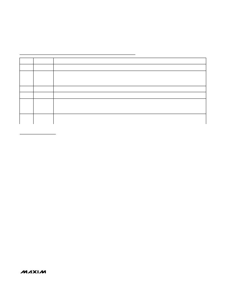
�PIN�
�11�
�12�
�13�
�14�
�15�
�16�
�NAME�
�AGND�
�CS�
�PGND�
�NDRV�
�V� CC�
�V� DD�
�FUNCTION�
�Analog� Ground.� Connect� to� PGND� close� to� the� IC.�
�Current� Sense� with� Blanking.� Turns� power� switch� off� if� V� CS� rises� above� 100mV� (referenced� to� PGND).�
�Connect� a� 100� ?� resistor� between� CS� and� the� current-sense� resistor� (Figure� 2).� Connect� CS� to� PGND� if�
�not� used.�
�Power� Ground.� Connect� to� AGND.�
�Gate� Drive� for� External� N-Channel� Power� FET�
�Output� Driver� Power-Rail� Decoupling� Point.� Connect� a� capacitor� to� PGND� with� half� the� value� used� for�
�V� DD� bypass� very� close� to� the� pin.� If� synchronizing� several� controllers,� power� the� fan-out� buffer� driving� the�
�FREQ� pins� from� this� pin.�
�9.75V� Internal� Linear-Regulator� Output.� Drive� V� DD� to� a� voltage� higher� than� 10.75V� to� bootstrap� the� chip�
�supply.� V� DD� is� also� the� supply� voltage� rail� for� the� chip.� Bypass� to� AGND� with� a� 5μF� to� 10μF� capacitor.�
�Detailed� Description�
�The� MAX5003� is� a� PWM� controller� designed� for� use� as�
�the� control� and� regulation� core� of� voltage-mode� control�
�flyback� converters� or� forward-voltage� power� convert-�
�ers.� It� provides� the� power-supply� designer� with� maxi-�
�mum� flexibility� and� ease� of� use.� The� device� is� specified�
�up� to� 110V� and� will� operate� from� as� low� as� 11V.� Its�
�maximum� operating� frequency� of� 300kHz� permits� the�
�use� of� miniature� magnetic� components� to� minimize�
�board� space.� The� range,� polarity,� and� range� of� output�
�voltages� and� power� are� limited� only� by� design� and� by�
�the� external� components� used.�
�This� device� works� in� isolated� and� nonisolated� configu-�
�rations,� and� in� applications� with� single� or� multiple� out-�
�put� voltages.� All� the� building� blocks� of� a� PWM�
�voltage-mode� controller� are� present� in� the� MAX5003�
�and� its� settings� are� adjustable.� The� functional� diagram�
�is� shown� on� Figure� 1.�
�Modern� Voltage-Mode� Controllers�
�The� MAX5003� offers� a� voltage-mode� control� topology�
�and� adds� features� such� as� fast� input� voltage� feed� for-�
�ward,� programmable� maximum� duty� cycle,� and� high�
�operating� frequencies.� It� has� all� the� advantages� of� cur-�
�rent-mode� control� —good� control� loop� bandwidth,�
�same-cycle� response� to� input� voltage� changes,� and�
�pulse-by-pulse� current� limiting.� It� eliminates� disadvan-�
�tages� such� as� the� need� for� ramp� compensation,� noise�
�sensitivity,� and� the� analytical� and� design� difficulties� of�
�dealing� with� two� nested� feedback� loops.� In� summary,�
�voltage-mode� control� has� inherent� superior� noise�
�immunity� and� uses� simpler� compensation� schemes.�
�Internal� Power� Regulators�
�The� MAX5003� ’s� power� stages� operate� over� a� wide�
�range� of� supply� voltages� while� maintaining� low� power�
�consumption.� For� the� high� end� of� the� range� (+36V� to�
�+110V),� power� is� fed� to� the� V+� pin� into� a� depletion�
�junction� FET� preregulator.� This� input� must� be� decou-�
�pled� with� a� 0.1μF� capacitor� to� the� power� ground� pin�
�(PGND).� To� decouple� the� power� line,� other� large-value�
�capacitors� must� be� placed� next� to� the� power� trans-�
�former� connection.�
�The� preregulator� drops� the� input� voltage� to� a� level� low�
�enough� to� feed� a� first� low-dropout� regulator� (LDO)�
�(Figure� 1).� The� input� to� the� LDO� is� brought� out� at� the� ES�
�pin.� ES� must� also� be� decoupled� with� a� 0.1μF� capacitor.�
�In� applications� where� the� maximum� input� voltage� is�
�below� 36V,� connect� ES� and� V+� together� and� decouple�
�with� a� 0.1μF� capacitor.�
�The� first� LDO� generates� the� power� for� the� V� DD� line.� The�
�V� DD� line� is� available� at� the� V� DD� pin� for� decoupling.� The�
�bypass� to� AGND� must� be� a� 5μF� to� 10μF� capacitor.�
�When� the� maximum� input� voltage� is� always� below�
�18.75V,� power� may� also� be� supplied� at� V� DD� ;� in� this�
�case,� connect� V+,� ES,� and� V� DD� together.�
�Forcing� voltages� at� V� DD� above� 10.75V� (see� Electrical�
�Characteristics� )� disables� the� first� LDO,� typically� reduc-�
�ing� current� consumption� below� 50μA� (see� Typical�
�Operating� Characteristics� ).�
�Following� the� V� DD� LDO� is� another� regulator� that� drives�
�V� CC� :� the� power� bus� for� the� internal� logic,� analog� cir-�
�cuitry,� and� external� power� MOSFET� driver.� This� regula-�
�tor� is� needed� because� the� V� DD� voltage� level� would� be�
�too� high� for� the� external� N-channel� MOSFET� gate.� The�
�_______________________________________________________________________________________�
�7�
�相关PDF资料 |
PDF描述 |
|---|---|
| VI-J44-EY-B1 | CONVERTER MOD DC/DC 48V 50W |
| MAX15005BAUE+ | IC REG CTRLR PWM CM 16-TSSOP |
| VI-JV0-EY-B1 | CONVERTER MOD DC/DC 5V 50W |
| UUE1H330MNS1GS | CAP ALUM 33UF 50V 20% SMD |
| UUE1E101MNS1GS | CAP ALUM 100UF 25V 20% SMD |
相关代理商/技术参数 |
参数描述 |
|---|---|
| MAX5003CSE+ | 功能描述:电压模式 PWM 控制器 PWM Power-Supply Controller RoHS:否 制造商:Texas Instruments 输出端数量:1 拓扑结构:Buck 输出电压:34 V 输出电流: 开关频率: 工作电源电压:4.5 V to 5.5 V 电源电流:600 uA 最大工作温度:+ 125 C 最小工作温度:- 40 C 封装 / 箱体:WSON-8 封装:Reel |
| MAX5003CSE+T | 功能描述:电压模式 PWM 控制器 PWM Power-Supply Controller RoHS:否 制造商:Texas Instruments 输出端数量:1 拓扑结构:Buck 输出电压:34 V 输出电流: 开关频率: 工作电源电压:4.5 V to 5.5 V 电源电流:600 uA 最大工作温度:+ 125 C 最小工作温度:- 40 C 封装 / 箱体:WSON-8 封装:Reel |
| MAX5003CSE-T | 功能描述:电压模式 PWM 控制器 PWM Power-Supply Controller RoHS:否 制造商:Texas Instruments 输出端数量:1 拓扑结构:Buck 输出电压:34 V 输出电流: 开关频率: 工作电源电压:4.5 V to 5.5 V 电源电流:600 uA 最大工作温度:+ 125 C 最小工作温度:- 40 C 封装 / 箱体:WSON-8 封装:Reel |
| MAX5003EEE | 功能描述:电压模式 PWM 控制器 PWM Power-Supply Controller RoHS:否 制造商:Texas Instruments 输出端数量:1 拓扑结构:Buck 输出电压:34 V 输出电流: 开关频率: 工作电源电压:4.5 V to 5.5 V 电源电流:600 uA 最大工作温度:+ 125 C 最小工作温度:- 40 C 封装 / 箱体:WSON-8 封装:Reel |
| MAX5003EEE+ | 功能描述:电压模式 PWM 控制器 PWM Power-Supply Controller RoHS:否 制造商:Texas Instruments 输出端数量:1 拓扑结构:Buck 输出电压:34 V 输出电流: 开关频率: 工作电源电压:4.5 V to 5.5 V 电源电流:600 uA 最大工作温度:+ 125 C 最小工作温度:- 40 C 封装 / 箱体:WSON-8 封装:Reel |
发布紧急采购,3分钟左右您将得到回复。