- 您现在的位置:买卖IC网 > PDF目录15152 > MAX5015CSA+T (Maxim Integrated Products)IC REG CTRLR ISO PWM CM 8-SOIC PDF资料下载
参数资料
| 型号: | MAX5015CSA+T |
| 厂商: | Maxim Integrated Products |
| 文件页数: | 6/14页 |
| 文件大小: | 0K |
| 描述: | IC REG CTRLR ISO PWM CM 8-SOIC |
| 产品培训模块: | Lead (SnPb) Finish for COTS Obsolescence Mitigation Program |
| 标准包装: | 2,500 |
| PWM 型: | 电流模式 |
| 输出数: | 1 |
| 频率 - 最大: | 275kHz |
| 占空比: | 50% |
| 电源电压: | 18 V ~ 110 V |
| 降压: | 无 |
| 升压: | 无 |
| 回扫: | 无 |
| 反相: | 无 |
| 倍增器: | 无 |
| 除法器: | 无 |
| Cuk: | 无 |
| 隔离: | 是 |
| 工作温度: | 0°C ~ 70°C |
| 封装/外壳: | 8-SOIC(0.154",3.90mm 宽) |
| 包装: | 带卷 (TR) |
�� �
�
�Current-Mode� PWM� Controllers� with� Integrated�
�Startup� Circuit� for� Isolated� Power� Supplies�
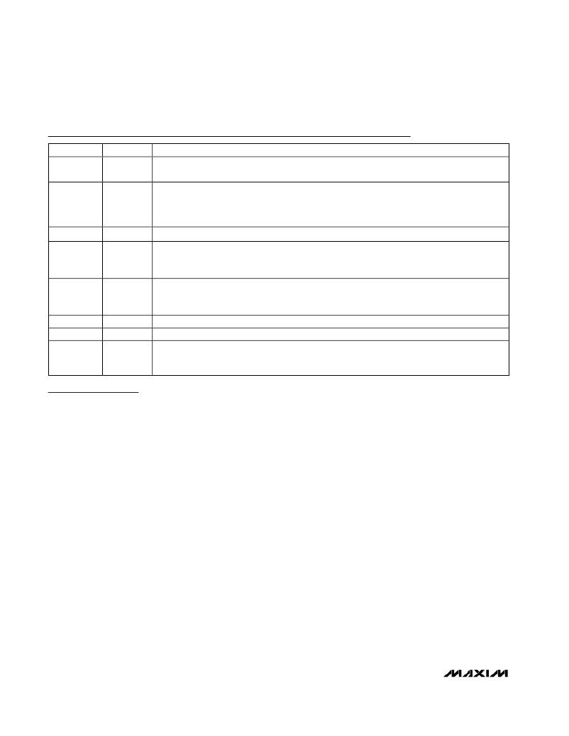
�Pin� Description�
�PIN�
�1�
�2�
�3�
�4�
�5�
�6�
�7�
�8�
�NAME�
�V+�
�V� DD�
�OPTO�
�SS_� SHDN�
�CS�
�GND�
�NDRV�
�V� CC�
�FUNCTION�
�High-Voltage� Startup� Input.� Connect� directly� to� an� input� voltage� between� 18V� to� 110V.� Connects�
�internally� to� a� high-voltage� linear� regulator� that� generates� V� CC� during� startup.�
�V� DD� is� the� Input� of� the� Linear� Regulator� that� Generates� V� CC� .� For� supply� voltages� less� than� 36V,� V� DD�
�and� V+� can� both� be� connected� to� the� supply.� For� supply� voltages� greater� than� 36V,� V� DD� receives�
�its� power� from� the� tertiary� winding� of� the� transformer� and� accepts� voltages� from� 13V� to� 36V.� Bypass�
�to� GND� with� a� 4.7μF� capacitor.�
�Optocoupler� Input.� The� control� voltage� range� on� this� input� is� 2V� to� 3V.�
�Soft-Start� Timing� Capacitor� Connection.� Ramp� time� to� full� current� limit� is� approximately� 0.45ms/nF.�
�This� pin� is� also� the� reference� voltage� output.� Bypass� with� a� minimum� 10nF� capacitor� to� GND.� The�
�device� goes� into� shutdown� when� V� SS_� SHDN� is� pulled� below� 0.25V.�
�Current� Sense� Input.� Turns� power� switch� off� if� V� CS� rises� above� 465mV� for� cycle-by-cycle� current�
�limiting.� CS� is� also� the� feedback� for� the� current-mode� controller.� CS� is� connected� to� the� PWM�
�comparator� through� a� leading� edge� blanking� circuit.�
�Ground�
�Gate� Drive.� Drives� a� high-voltage� external� N-channel� power� MOSFET.�
�Regulated� IC� Supply.� Provides� power� for� the� entire� IC.� V� CC� is� regulated� from� V� DD� during� normal�
�operation� and� from� V+� during� startup.� Bypass� V� CC� with� a� 10� μ� F� tantalum� capacitor� in� parallel� with�
�0.1μF� ceramic� capacitor� to� GND.�
�Detailed� Description�
�Use� the� MAX5014/MAX5015� PWM� current-mode� con-�
�trollers� to� design� flyback-� or� forward-mode� power� sup-�
�plies.� Current-mode� operation� simplifies� control-loop�
�design� while� enhancing� loop� stability.� An� internal� high-�
�voltage� startup� regulator� allows� the� device� to� connect�
�directly� to� the� input� supply� without� an� external� startup�
�resistor.� Current� from� the� internal� regulator� starts� the�
�controller.� Once� the� tertiary� winding� voltage� is� estab-�
�lished� the� internal� regulator� is� switched� off� and� bias�
�current� for� running� the� IC� is� derived� from� the� tertiary�
�winding.� The� internal� oscillator� is� set� to� 275kHz� and�
�trimmed� to� ±10%.� This� permits� the� use� of� small� mag-�
�netic� components� to� minimize� board� space.� Both� the�
�MAX5014� and� MAX5015� can� be� used� in� power� sup-�
�plies� providing� multiple� output� voltages.� A� functional�
�diagram� of� the� IC� is� shown� in� Figure� 1.� Typical� applica-�
�tions� circuits� for� forward� and� flyback� topologies� are�
�shown� in� Figure� 2� and� Figure� 3,� respectively.�
�Current-Mode� Control�
�The� MAX5014/MAX5015� offer� current-mode� control�
�operation� with� added� features� such� as� leading-edge�
�blanking� with� dual� internal� path� that� only� blanks� the�
�sensed� current� signal� applied� to� the� input� of� the� PWM�
�comparator.� The� current� limit� comparator� monitors� the�
�CS� pin� at� all� times� and� provides� cycle-by-cycle� current�
�limit� without� being� blanked.� The� leading-edge� blanking�
�of� the� CS� signal� prevents� the� PWM� comparator� from�
�prematurely� terminating� the� on� cycle.� The� CS� signal�
�contains� a� leading-edge� spike� that� is� the� result� of� the�
�MOSFET� gate� charge� current,� capacitive� and� diode�
�reverse� recovery� current� of� the� power� circuit.� Since� this�
�leading-edge� spike� is� normally� lower� than� the� current�
�limit� comparator� threshold,� current� limiting� is� not�
�blanked� and� cycle-by-cycle� current� limiting� is� provided�
�under� all� conditions.�
�Use� the� MAX5014� in� discontinuous� flyback� applications�
�where� wide� line� voltage� and� load� current� variation� is�
�expected.� Use� the� MAX5015� for� single� transistor� for-�
�ward� converters� where� the� maximum� duty� cycle� must�
�be� limited� to� less� than� 50%.�
�Under� certain� conditions� it� may� be� advantageous� to�
�use� a� forward� converter� with� greater� than� 50%� duty�
�cycle.� For� those� cases� use� the� MAX5014.� The� large�
�duty� cycle� results� in� much� lower� operating� primary�
�RMS� currents� through� the� MOSFET� switch� and� in� most�
�cases� a� smaller� output� filter� inductor.� The� major� disad-�
�vantage� to� this� is� that� the� MOSFET� voltage� rating� must�
�be� higher� and� that� slope� compensation� must� be� provid-�
�ed� to� stabilize� the� inner� current� loop.� The� MAX5014�
�provides� internal� slope� compensation.�
�6�
�_______________________________________________________________________________________�
�相关PDF资料 |
PDF描述 |
|---|---|
| MAX5019CSA+T | IC REG CTRLR FLYBK ISO PWM 8SOIC |
| MAX5019ESA+T | IC REG CTRLR FLYBK ISO PWM 8SOIC |
| MAX5014CSA+T | IC REG CTRLR FLYBK ISO PWM 8SOIC |
| MAX5014ESA+T | IC REG CTRLR FLYBK ISO PWM 8SOIC |
| ABB13DHHD | CONN EDGECARD 26POS .050 DIP SLD |
相关代理商/技术参数 |
参数描述 |
|---|---|
| MAX5015ESA | 功能描述:电流型 PWM 控制器 w/Integrated Startup RoHS:否 制造商:Texas Instruments 开关频率:27 KHz 上升时间: 下降时间: 工作电源电压:6 V to 15 V 工作电源电流:1.5 mA 输出端数量:1 最大工作温度:+ 105 C 安装风格:SMD/SMT 封装 / 箱体:TSSOP-14 |
| MAX5015ESA+ | 功能描述:电流型 PWM 控制器 w/Integrated Startup RoHS:否 制造商:Texas Instruments 开关频率:27 KHz 上升时间: 下降时间: 工作电源电压:6 V to 15 V 工作电源电流:1.5 mA 输出端数量:1 最大工作温度:+ 105 C 安装风格:SMD/SMT 封装 / 箱体:TSSOP-14 |
| MAX5015ESA+T | 功能描述:电流型 PWM 控制器 w/Integrated Startup RoHS:否 制造商:Texas Instruments 开关频率:27 KHz 上升时间: 下降时间: 工作电源电压:6 V to 15 V 工作电源电流:1.5 mA 输出端数量:1 最大工作温度:+ 105 C 安装风格:SMD/SMT 封装 / 箱体:TSSOP-14 |
| MAX5015ESA-G077 | 功能描述:电流型 PWM 控制器 RoHS:否 制造商:Texas Instruments 开关频率:27 KHz 上升时间: 下降时间: 工作电源电压:6 V to 15 V 工作电源电流:1.5 mA 输出端数量:1 最大工作温度:+ 105 C 安装风格:SMD/SMT 封装 / 箱体:TSSOP-14 |
| MAX5015ESA-T | 功能描述:电流型 PWM 控制器 w/Integrated Startup RoHS:否 制造商:Texas Instruments 开关频率:27 KHz 上升时间: 下降时间: 工作电源电压:6 V to 15 V 工作电源电流:1.5 mA 输出端数量:1 最大工作温度:+ 105 C 安装风格:SMD/SMT 封装 / 箱体:TSSOP-14 |
发布紧急采购,3分钟左右您将得到回复。