- 您现在的位置:买卖IC网 > PDF目录14396 > MAX5035BUPA+ (Maxim Integrated Products)IC REG BUCK 5V 1A 8DIP PDF资料下载
参数资料
| 型号: | MAX5035BUPA+ |
| 厂商: | Maxim Integrated Products |
| 文件页数: | 10/17页 |
| 文件大小: | 0K |
| 描述: | IC REG BUCK 5V 1A 8DIP |
| 产品培训模块: | Lead (SnPb) Finish for COTS Obsolescence Mitigation Program |
| 标准包装: | 50 |
| 类型: | 降压(降压) |
| 输出类型: | 固定 |
| 输出数: | 1 |
| 输出电压: | 5V |
| 输入电压: | 7.5 V ~ 76 V |
| PWM 型: | 电压模式 |
| 频率 - 开关: | 125kHz |
| 电流 - 输出: | 1A |
| 同步整流器: | 无 |
| 工作温度: | 0°C ~ 85°C |
| 安装类型: | 通孔 |
| 封装/外壳: | 8-DIP(0.300",7.62mm) |
| 包装: | 管件 |
| 供应商设备封装: | 8-PDIP |
�� �
�
�MAX5035�
�1A,� 76V,� High-Efficiency� MAXPower�
�Step-Down� DC-DC� Converter�
�Detailed� Description�
�The� MAX5035� step-down� DC-DC� converter� operates�
�from� a� 7.5V� to� 76V� input� voltage� range.� A� unique� volt-�
�age-mode� control� scheme� with� voltage� feed-forward�
�and� an� internal� switching� DMOS� FET� provides� high� effi-�
�ciency� over� a� wide� input� voltage� range.� This� pulse-�
�width� modulated� converter� operates� at� a� fixed� 125kHz�
�switching� frequency.� The� device� also� features� automat-�
�ic� pulse-skipping� mode� to� provide� low� quiescent� cur-�
�rent� and� high� efficiency� at� light� loads.� Under� no� load,�
�the� MAX5035� consumes� only� 270μA,� and� in� shutdown�
�mode,� consumes� only� 10μA.� The� MAX5035� also� fea-�
�tures� undervoltage� lockout,� hiccup� mode� output� short-�
�circuit� protection,� and� thermal� shutdown.�
�Shutdown� Mode�
�Drive� ON/� OFF� to� ground� to� shut� down� the� MAX5035.�
�Shutdown� forces� the� internal� power� MOSFET� off,� turns�
�off� all� internal� circuitry,� and� reduces� the� V� IN� supply� cur-�
�rent� to� 10μA� (typ).� The� ON/� OFF� rising� threshold� is�
�1.69V� (typ).� Before� any� operation� begins,� the� voltage� at�
�ON/� OFF� must� exceed� 1.69V� (typ).� The� ON/� OFF� input�
�has� 100mV� hysteresis.�
�Undervoltage� Lockout� (UVLO)�
�Use� the� ON/� OFF� function� to� program� the� UVLO� thresh-�
�old� at� the� input.� Connect� a� resistive� voltage-divider�
�from� V� IN� to� GND� with� the� center� node� to� ON/� OFF� as�
�shown� in� Figure� 1.� Calculate� the� threshold� value� by�
�using� the� following� formula:�
�On� startup,� an� internal� low-side� switch� connects� LX� to�
�ground� and� charges� the� BST� capacitor� to� VD.� Once� the�
�BST� capacitor� is� charged,� the� internal� low-side� switch�
�is� turned� off� and� the� BST� capacitor� voltage� provides�
�the� necessary� enhancement� voltage� to� turn� on� the�
�high-side� switch.�
�Thermal-Overload� Protection�
�The� MAX5035� features� integrated� thermal� overload� pro-�
�tection.� Thermal� overload� protection� limits� total� power�
�dissipation� in� the� device,� and� protects� the� device� in� the�
�event� of� a� fault� condition.� When� the� die� temperature�
�exceeds� +160°C,� an� internal� thermal� sensor� signals� the�
�shutdown� logic,� turning� off� the� internal� power� MOSFET�
�and� allowing� the� IC� to� cool.� The� thermal� sensor� turns� the�
�internal� power� MOSFET� back� on� after� the� IC’s� die� tem-�
�perature� cools� down� to� +140°C,� resulting� in� a� pulsed�
�output� under� continuous� thermal� overload� conditions.�
�Applications� Information�
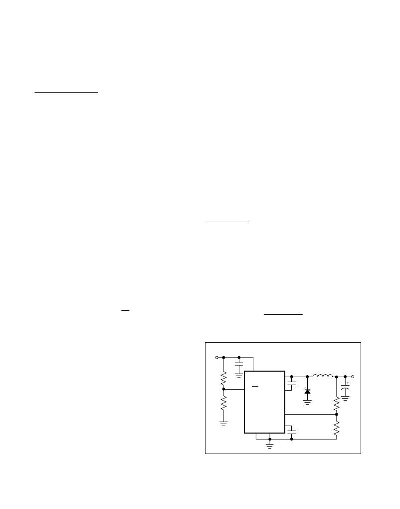
�Setting� the� Output� Voltage�
�The� MAX5035A/B/C� have� preset� output� voltages� of� 3.3V,�
�5.0V,� and� 12V,� respectively.� Connect� FB� to� the� preset�
�output� voltage� (see� the� Typical� Operating� Circuit).�
�The� MAX5035D/E� versions� offer� an� adjustable� output�
�voltage.� Set� the� output� voltage� with� a� resistive� voltage-�
�divider� connected� from� the� circuit’s� output� to� ground�
�(Figure� 1).� Connect� the� center� node� of� the� divider� to�
�FB.� Choose� R4� less� than� 15k� ?� ,� then� calculate� R3� as�
�follows:�
�V� UVLO� (� TH� )� =� ?� 1� +�
�?�
�?�
�R1� ?�
�R� 2� ?� ?�
�� 1� .� 85� V�
�R� 3� =�
�(V� OUT� ?� 1 . 22)�
�1� .� 22�
�� R� 4�
�The� minimum� recommended� V� UVLO(TH)� is� 6.5V,� 7.5V,� and�
�13V� for� the� output� voltages� of� 3.3V,� 5V,� and� 12V,� respec-�
�tively.� The� recommended� value� for� R2� is� less� than� 1M� ?� .�
�If� the� external� UVLO� threshold-setting� divider� is� not�
�V� IN�
�7.5V� TO� 76V�
�used,� an� internal� undervoltage-lockout� feature� monitors�
�the� supply� voltage� at� V� IN� and� allows� operation� to� start�
�when� V� IN� rises� above� 5.2V� (typ).� This� feature� can� be�
�used� only� when� V� IN� rise� time� is� faster� than� 2ms.� For�
�slower� V� IN� rise� time,� use� the� resistive-divider� at�
�ON/� OFF� .�
�R1�
�68� μ� F�
�V� IN�
�ON/OFF�
�LX�
�BST�
�0.1� μ� F�
�100� μ� H�
�D1�
�50SQ100�
�V� OUT�
�5V�
�C� OUT�
�68� μ� F�
�Boost� High-Side� Gate� Drive� (BST)�
�Connect� a� flying� bootstrap� capacitor� between� LX� and�
�R2�
�MAX5035D�
�FB�
�R3�
�41.2k� ?�
�BST� to� provide� the� gate-drive� voltage� to� the� high-side�
�N-channel� DMOS� switch.� The� capacitor� is� alternately�
�charged� from� the� internally� regulated� output� voltage� VD�
�SGND�
�GND�
�VD�
�0.1� μ� F�
�R4�
�13.3k� ?�
�and� placed� across� the� high-side� DMOS� driver.� Use� a�
�0.1μF,� 16V� ceramic� capacitor� located� as� close� to� the�
�device� as� possible.�
�10�
�Figure� 1.� Adjustable� Output� Voltage�
�Maxim� Integrated�
�相关PDF资料 |
PDF描述 |
|---|---|
| MAX5035DUPA+ | IC REG BUCK ADJ 1A 8DIP |
| LTC3620EDC#TRMPBF | IC REG BUCK SYNC ADJ 15MA 8DFN |
| RSM22DSEN | CONN EDGECARD 44POS .156 EYELET |
| GSM22DRMT | CONN EDGECARD 44POS .156 WW |
| GMM22DRMT | CONN EDGECARD 44POS .156 WW |
相关代理商/技术参数 |
参数描述 |
|---|---|
| MAX5035BUPA+ | 功能描述:直流/直流开关转换器 1A 76V MAXPower Step-Down RoHS:否 制造商:STMicroelectronics 最大输入电压:4.5 V 开关频率:1.5 MHz 输出电压:4.6 V 输出电流:250 mA 输出端数量:2 最大工作温度:+ 85 C 安装风格:SMD/SMT |
| MAX5035BUPA+T | 制造商:Maxim Integrated Products 功能描述:- Tape and Reel |
| MAX5035BUSA | 功能描述:直流/直流开关转换器 1A 76V MAXPower Step-Down RoHS:否 制造商:STMicroelectronics 最大输入电压:4.5 V 开关频率:1.5 MHz 输出电压:4.6 V 输出电流:250 mA 输出端数量:2 最大工作温度:+ 85 C 安装风格:SMD/SMT |
| MAX5035BUSA+ | 功能描述:直流/直流开关转换器 1A 76V MAXPower Step-Down RoHS:否 制造商:STMicroelectronics 最大输入电压:4.5 V 开关频率:1.5 MHz 输出电压:4.6 V 输出电流:250 mA 输出端数量:2 最大工作温度:+ 85 C 安装风格:SMD/SMT |
| MAX5035BUSA+T | 功能描述:直流/直流开关转换器 1A 76V MAXPower Step-Down RoHS:否 制造商:STMicroelectronics 最大输入电压:4.5 V 开关频率:1.5 MHz 输出电压:4.6 V 输出电流:250 mA 输出端数量:2 最大工作温度:+ 85 C 安装风格:SMD/SMT |
发布紧急采购,3分钟左右您将得到回复。