- 您现在的位置:买卖IC网 > PDF目录17280 > MAX5042EVKIT (Maxim Integrated Products)EVAL KIT FOR MAX5042 PDF资料下载
参数资料
| 型号: | MAX5042EVKIT |
| 厂商: | Maxim Integrated Products |
| 文件页数: | 13/22页 |
| 文件大小: | 0K |
| 描述: | EVAL KIT FOR MAX5042 |
| 产品培训模块: | Lead (SnPb) Finish for COTS Obsolescence Mitigation Program |
| 标准包装: | 1 |
| 主要目的: | DC/DC,步降 |
| 输出及类型: | 1,隔离 |
| 输出电压: | 5V |
| 电流 - 输出: | 8A |
| 输入电压: | ±36 V ~ 75 V |
| 稳压器拓扑结构: | 降压 |
| 频率 - 开关: | 250kHz |
| 板类型: | 完全填充 |
| 已供物品: | 板 |
| 已用 IC / 零件: | MAX5042 |
�� �
�
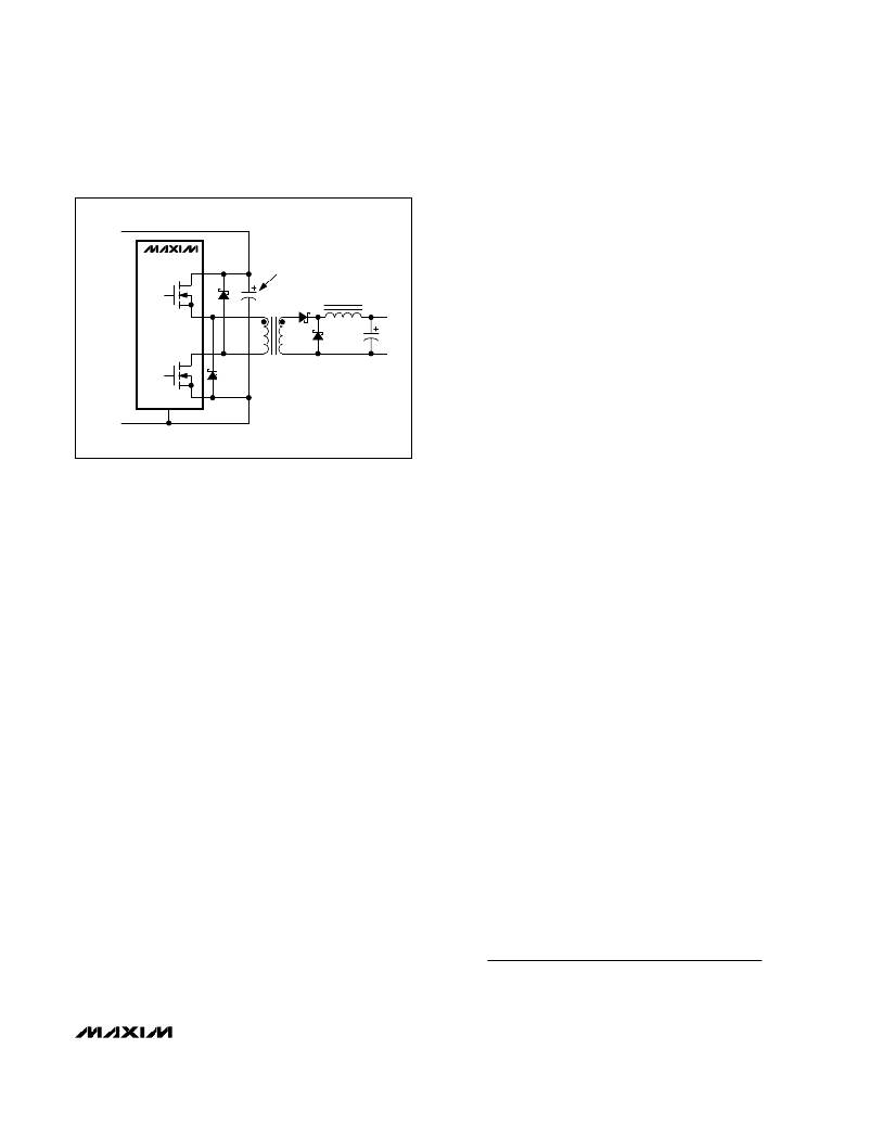
�Two-Switch� Power� ICs� with� Integrated�
�Power� MOSFETs� and� Hot-Swap� Controller�
�Power� Topology�
�The� two-switch� forward-converter� topology� offers� out-�
�+V� POSINPWM�
�standing� robustness� against� faults� and� transformer� satu-�
�MAX5043�
�QH�
�C� IN�
�BULK� STORAGE� CAPACITOR�
�L�
�ration� while� affording� efficient� use� of� the� integrated�
�75m� ?� power� MOSFETs.� Voltage-mode� control� with� feed-�
�forward� compensation� allows� the� rejection� of� input� sup-�
�ply� disturbances� within� a� single� cycle� similar� to� that� of�
�QL�
�PWM�
�CIRCUIT�
�WITH�
�INTEGRATED�
�FETs�
�T1�
�V� OUT�
�C� OUT�
�current-mode� controlled� topologies.� This� control� method�
�offers� some� significant� benefits� when� compared� with�
�current-mode� control.� These� benefits� include:�
�?� No� minimum� duty-cycle� requirement� due� to� current-�
�signal� filtering� or� blanking.�
�?� Clean� modulator� ramp� and� higher� amplitude� for�
�increased� stability.�
�PWMNEG�
�Figure� 2.� Simplified� Diagram� of� a� MAX5043-Based� Isolated�
�Power� Supply�
�Set� the� switching� frequency� with� a� resistor� and� a�
�capacitor� at� RCOSC.� Switching� at� 250kHz� ensures�
�switching� losses� are� minimal� and� external� power� pas-�
�sives� are� small� enough� for� a� compact� circuit.�
�The� MAX5042/MAX5043� incorporate� an� advanced� set� of�
�protection� features� that� make� them� uniquely� suitable�
�when� high� reliability� and� comprehensive� fault� protection�
�are� required,� as� in� telecommunication� equipment� power-�
�supply� applications.� The� MAX5042/MAX5043� 15V� linear�
�regulator� output� powers� the� 9V� and� 5V� regulators� used� to�
�drive� the� gates� and� internal� circuitry.� A� tertiary� winding�
�connects� to� REG15� through� a� rectifier� to� power� the�
�device� after� startup� and� reduces� power� dissipation� in� the�
�MAX5042/MAX5043� package.� When� REG15� is� externally�
�powered,� the� internal� 15V� regulator� is� disabled.�
�Figures� 3� and� 4� show� the� block� diagrams� of� the� MAX5042�
�and� MAX5043,� respectively.� The� power-OK� signals� from�
�the� hot-swap� section,� regulators,� thermal� shutdown,� and�
�UVLO� combine� to� generate� the� internal� shutdown� signal�
�SHDN.� When� asserted,� SHDN� disables� the� comparators�
�and� oscillator.� Deasserting� SHDN� releases� the� compara-�
�tors� and� oscillators.� The� falling� edge� of� SHDN� is� delayed�
�allowing� the� internal� signals� to� settle� before� the� PWM� puls-�
�es� appear.� During� the� time� between� the� falling� edge� of�
�SHDN� and� its� delayed� signal,� the� 10� ?� internal� MOSFET�
�(QB)� from� XFRMRH� to� PWMPNEG� turns� on,� charging� the�
�BST� capacitor.� After� startup,� this� MOSFET� also� turns� on�
�for� approximately� 300ns� at� each� half� period� to� help�
�?� Stable� bias� point� of� the� optocoupler� LED� and� photo-�
�transistor� for� maximized� control-loop� bandwidth� (in�
�current-mode� applications,� the� optocoupler� bias�
�point� is� output-load� dependent).�
�?� Predictable� loop� dynamics� simplifying� the� design� of�
�the� control� loop.�
�The� two-switch� power� topology� recovers� energy� stored�
�in� both� the� magnetizing� and� parasitic� leakage� induc-�
�tances� of� the� transformer.� Figure� 7� shows� the� schemat-�
�ic� diagram� of� a� 48V� input� and� 5V,� 8A� output� isolated�
�power� supply� built� with� the� MAX5042.�
�The� MAX5042/MAX5043� also� support� current-mode� con-�
�trol.� Current-mode� control� has� advantages� such� as� a� sin-�
�gle-pole� power� circuit� and� a� small-signal� transfer�
�function� that� simplify� the� design� of� power� supplies� with�
�widely� varying� output� capacitors.�
�Undervoltage� Lockout�
�The� MAX5042� has� two� UVLO� functions.� Both� the� hot-�
�swap� section� and� the� PWM� section� contain� their� own�
�undervoltage� lockout� comparators� (HSEN� and� UVLO,�
�respectively).� The� MAX5043� lacks� the� hot-swapping�
�function,� but� retains� the� PWM� UVLO� and� the� deglitched�
�undervoltage� lockout/power-on� reset.� In� both� cases,�
�internal� resistors� set� a� default� input-voltage� enable�
�threshold� of� 31V� (typ).�
�The� PWM� default� input� voltage� threshold� value� can� be�
�adjusted� by� using� an� external� divider� in� parallel� with� the�
�internal� divider.� The� tolerances� of� the� external� divider�
�resistors� dominate� the� precision� of� the� UVLO� trip� point� if�
�their� values� are� smaller� than� those� of� the� internal� divider.�
�Override� the� default� threshold� by� using:�
�charge� the� BST� capacitor.�
�R� He� =�
�R� Le� � R� Li� � R� Hi� � (� V� IN� -� V� REF� )�
�V� REF� � R� Hi� (� R� Li� +� R� Le� )� -� R� Le� � R� Li� � (� V� IN� -� V� REF� )�
�______________________________________________________________________________________�
�13�
�相关PDF资料 |
PDF描述 |
|---|---|
| 050R18-102B | CABLE FLAT FLEX 18POS 0.5MM 4" |
| MAX5066EVKIT | EVAL KIT FOR MAX5066 |
| L-14C27NJV4T | CER INDUCTOR 27NH 0603 |
| MC33385VW | IC SWITCH QUAD L-SIDE 20-HSOP |
| MC33186VW1 | IC DRIVER H-BRIDGE 20-HSOP |
相关代理商/技术参数 |
参数描述 |
|---|---|
| MAX5043ATN+ | 制造商:Maxim Integrated Products 功能描述:- Rail/Tube |
| MAX5043ETN | 功能描述:开关变换器、稳压器与控制器 Two-Switch Power IC w/Power MOSFET RoHS:否 制造商:Texas Instruments 输出电压:1.2 V to 10 V 输出电流:300 mA 输出功率: 输入电压:3 V to 17 V 开关频率:1 MHz 工作温度范围: 安装风格:SMD/SMT 封装 / 箱体:WSON-8 封装:Reel |
| MAX5043ETN+ | 功能描述:开关变换器、稳压器与控制器 Two-Switch Power IC w/Power MOSFET RoHS:否 制造商:Texas Instruments 输出电压:1.2 V to 10 V 输出电流:300 mA 输出功率: 输入电压:3 V to 17 V 开关频率:1 MHz 工作温度范围: 安装风格:SMD/SMT 封装 / 箱体:WSON-8 封装:Reel |
| MAX5043ETN+T | 功能描述:开关变换器、稳压器与控制器 Two-Switch Power IC w/Power MOSFET RoHS:否 制造商:Texas Instruments 输出电压:1.2 V to 10 V 输出电流:300 mA 输出功率: 输入电压:3 V to 17 V 开关频率:1 MHz 工作温度范围: 安装风格:SMD/SMT 封装 / 箱体:WSON-8 封装:Reel |
| MAX5043ETN-T | 功能描述:开关变换器、稳压器与控制器 Two-Switch Power IC w/Power MOSFET RoHS:否 制造商:Texas Instruments 输出电压:1.2 V to 10 V 输出电流:300 mA 输出功率: 输入电压:3 V to 17 V 开关频率:1 MHz 工作温度范围: 安装风格:SMD/SMT 封装 / 箱体:WSON-8 封装:Reel |
发布紧急采购,3分钟左右您将得到回复。