- 您现在的位置:买卖IC网 > PDF目录8522 > MAX504ESD+T (Maxim Integrated Products)IC DAC 10BIT VOLT OUT 14-SOIC PDF资料下载
参数资料
| 型号: | MAX504ESD+T |
| 厂商: | Maxim Integrated Products |
| 文件页数: | 16/16页 |
| 文件大小: | 0K |
| 描述: | IC DAC 10BIT VOLT OUT 14-SOIC |
| 产品培训模块: | Lead (SnPb) Finish for COTS Obsolescence Mitigation Program |
| 标准包装: | 2,500 |
| 设置时间: | 25µs |
| 位数: | 10 |
| 数据接口: | 串行 |
| 转换器数目: | 1 |
| 电压电源: | 单电源 |
| 工作温度: | -40°C ~ 85°C |
| 安装类型: | 表面贴装 |
| 封装/外壳: | 14-SOIC(0.154",3.90mm 宽) |
| 供应商设备封装: | 14-SOIC |
| 包装: | 带卷 (TR) |
| 输出数目和类型: | 1 电压,单极;1 电压,双极 |
| 采样率(每秒): | * |
Internal Reference (MAX504 only)
The on-chip reference is laser trimmed to generate 2.048V
at REFOUT. The output stage can source and sink current
so REFOUT can settle to the correct voltage quickly in
response to code-dependent loading changes. Typically,
source current is 5mA and sink current is 100A.
REFOUT connects the internal reference to the R-2R DAC
ladder at REFIN. The R-2R ladder draws 50A maximum
load current. If any other connection is made to REFOUT,
ensure that the total load current is less than 100A to
avoid gain errors.
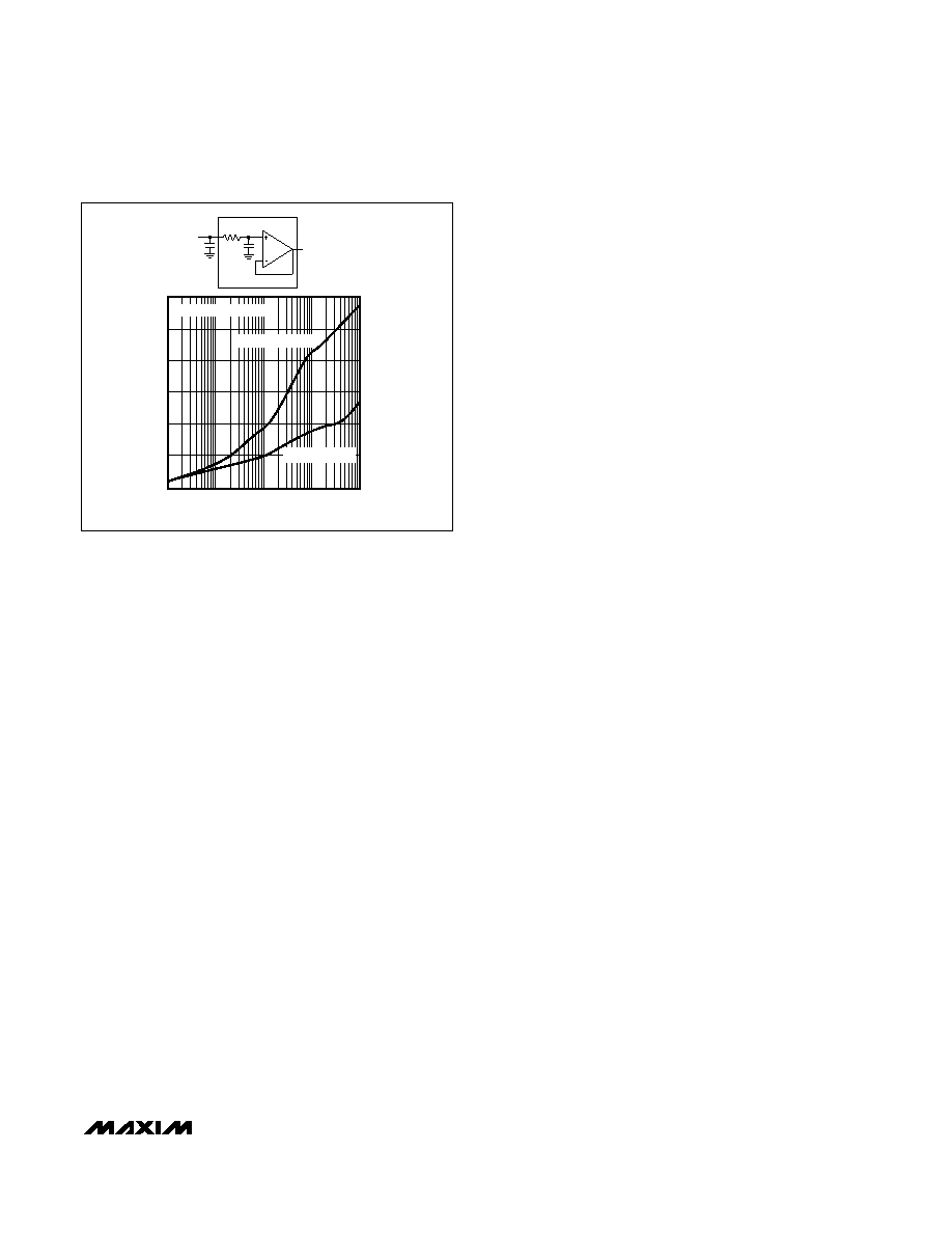
For applications requiring very low-noise performance, con-
nect a 33F capacitor from REFOUT to AGND. If noise is
not a concern, a lower value (3.3F min) capacitor may be
used. To reduce noise further, insert a buffered RC filter
between REFOUT and REFIN (Figure 2). The reference
bypass capacitor CREFOUT is still required for reference sta-
bility. In applications not requiring the reference, connect
REFOUT to VDD (to save power and to eliminate the need
for CREFOUT) or use the MAX515 (no internal reference).
External Reference
An external reference in the range (VSS + 2V) to (VDD - 2V)
may be used with the MAX504 in dual-supply operation.
With the MAX515 or the MAX504 in single-supply use, the
reference must be positive and may not exceed VDD - 2V.
The reference voltage determines the DAC’s full-scale out-
put. The DAC input resistance is code dependent and is
minimum (40k
) at code 0101... and virtually infinite at
code 0000.... REFIN’s input capacitance is also code
dependent and has a 50pF maximum value at several
codes.
If an upgrade to the internal reference is required, the 2.5V
MAX873A is suitable: ±15mV initial accuracy, TCVOUT =
7ppm/°C (max).
Logic Interface
The MAX504/MAX515 logic inputs are designed to be
compatible with TTL or CMOS logic levels. However, to
achieve the lowest power dissipation, drive the digital
inputs with rail-to-rail CMOS logic. With TTL logic levels,
the power requirement increases by a factor of approxi-
mately 2.
Serial Clock and Update Rate
Figure 1 shows the MAX504/MAX515 timing. The maxi-
mum serial clock rate is given by 1/(tCH+tCL), approxi-
mately 14MHz. The digital update rate is limited by the
chip-select period, which is 16 x (tCH + tCL) + tCSW.
This equals a 1.14s, or 877kHz, update rate. However,
the DAC settling time to 10 bits is 25s, which may limit
the update rate to 40kHz for full-scale step transitions.
____________Applications Information
Refer to Figures 3a and 3b for typical operating con-
nections.
Serial Interface
The MAX504/MAX515 use a three-wire serial interface that
is compatible with SPI, QSPI (CPOL = CPHA = 0), and
Microwire standards as shown in Figures 4 and 5. The
DAC is programmed by writing two 8-bit words (see Figure
1 and the
Functional Diagram). 16 bits of serial data are
clocked into the DAC in the following order: 4 fill (dummy)
bits, 10 data bits, and 2 sub-LSB 0s. The 4 dummy bits are
not normally needed, and are required only when DACs
are daisy chained. The 2 sub-LSB 0s, however, are always
needed, and allow hardware and software compatibility
with the 12-bit MAX531/MAX538/MAX539. Transitions at
CS should occur while SCLK is low. Data is clocked in on
SCLK’s rising edge while CS is low. The serial input data is
held in a 16-bit serial shift register. On CS’s rising edge, the
10 data-bits are transferred to the DAC register and update
the DAC. With CS high, data cannot be clocked into the
MAX504/MAX514.
The MAX504/MAX515 inputs data in 16-bit blocks. The SPI
and Microwire interfaces output data in 8-bit blocks, there-
by requiring two write cycles to input data to the DAC. The
QSPI interface allows variable data input from 8 to 16 bits,
and can be loaded into the DAC in one write cycle.
MAX504/MAX515
5V, Low-Power, Voltage-Output,
Serial 10-Bit DACs
_______________________________________________________________________________________
9
300
50
1
10
100
MAX504-FIG02
FREQUENCY (kHz)
REFERENCE
NOISE
(
V
RMS
)
150
200
250
0
0.1
1000
TOTAL
REFERENCE
NOISE
RS
REFOUT
CREFOUT
CS
TEK 7A22
CREFOUT = 3.3F
CREFOUT = 47F
SINGLE POLE ROLLOFF
1.8
1.6
1.4
1.2
1.0
0.8
0.6
0.4
0.2
0.0
REFERENCE
NOISE
(mVp-p)
Figure 2. Reference Noise vs. Frequency
SPI and QSPI are trademarks of Motorola, Inc. Microwire is a trademark of National Semiconductor Corp.
相关PDF资料 |
PDF描述 |
|---|---|
| VI-BNL-MU-F3 | CONVERTER MOD DC/DC 28V 200W |
| VI-BNL-MU-F2 | CONVERTER MOD DC/DC 28V 200W |
| VI-BNL-MU-F1 | CONVERTER MOD DC/DC 28V 200W |
| MAX9652ASA+T | IC AMP FILTER W/SHUTDOWN 8-SOIC |
| MAX4389EXT+T | IC OP AMP 85MHZ R-R SC70-6 |
相关代理商/技术参数 |
参数描述 |
|---|---|
| MAX505 | 制造商:MAXIM 制造商全称:Maxim Integrated Products 功能描述:Quad 8-Bit DACs with Rail-to-Rail Voltage Outputs |
| MAX505/MAX506 | 制造商:MAXIM 制造商全称:Maxim Integrated Products 功能描述:Quad 8-Bit DACs with Rail-to Rail Voltage Outputs |
| MAX5051 | 制造商:MAXIM 制造商全称:Maxim Integrated Products 功能描述:Parallelable, Clamped Two-Switch Power-Supply Controller IC |
| MAX5051AAUI+ | 功能描述:开关变换器、稳压器与控制器 RoHS:否 制造商:Texas Instruments 输出电压:1.2 V to 10 V 输出电流:300 mA 输出功率: 输入电压:3 V to 17 V 开关频率:1 MHz 工作温度范围: 安装风格:SMD/SMT 封装 / 箱体:WSON-8 封装:Reel |
| MAX5051AAUI+T | 功能描述:开关变换器、稳压器与控制器 RoHS:否 制造商:Texas Instruments 输出电压:1.2 V to 10 V 输出电流:300 mA 输出功率: 输入电压:3 V to 17 V 开关频率:1 MHz 工作温度范围: 安装风格:SMD/SMT 封装 / 箱体:WSON-8 封装:Reel |
发布紧急采购,3分钟左右您将得到回复。