- 您现在的位置:买卖IC网 > Datasheet目录341 > MAX5078BATT+T (Maxim Integrated Products)IC MOSFET DRIVER 6-TDFN Datasheet资料下载
参数资料
| 型号: | MAX5078BATT+T |
| 厂商: | Maxim Integrated Products |
| 文件页数: | 8/13页 |
| 文件大小: | 0K |
| 描述: | IC MOSFET DRIVER 6-TDFN |
| 产品培训模块: | Lead (SnPb) Finish for COTS Obsolescence Mitigation Program |
| 标准包装: | 1 |
| 配置: | 低端 |
| 输入类型: | 反相和非反相 |
| 延迟时间: | 20ns |
| 电流 - 峰: | 4A |
| 配置数: | 1 |
| 输出数: | 1 |
| 电源电压: | 4 V ~ 15 V |
| 工作温度: | -40°C ~ 125°C |
| 安装类型: | 表面贴装 |
| 封装/外壳: | 6-WDFN 裸露焊盘 |
| 供应商设备封装: | 6-TDFN 裸露焊盘(3x3) |
| 包装: | 标准包装 |
| 产品目录页面: | 1411 (CN2011-ZH PDF) |
| 其它名称: | MAX5078BATT+TDKR |
�� �
�
�MAX5078�
�4A,� 20ns,� MOSFET� Driver�
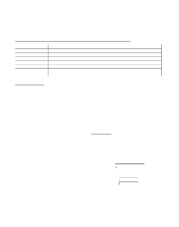
�Pin� Description�
�PIN�
�1�
�2,� 3�
�4�
�5�
�6�
�—�
�NAME�
�IN-�
�GND�
�V� DD�
�OUT�
�IN+�
�EP�
�FUNCTION�
�Inverting� Logic-Input� Terminal.� Connect� to� GND� when� not� used.�
�Ground�
�Power� Supply.� Bypass� to� GND� with� one� or� more� 0.1μF� ceramic� capacitors.�
�Driver� Output.� Sources� or� sinks� current� to� turn� the� external� MOSFET� on� or� off.�
�Noninverting� Logic-Input� Terminal.� Connect� to� V� DD� when� not� used.�
�Exposed� Pad.� Internally� connected� to� GND.� Do� not� use� the� exposed� pad� as� the� only� electrical�
�ground� connection.�
�Detailed� Description�
�V� DD� Undervoltage� Lockout� (UVLO)�
�The� MAX5078A/MAX5078B� have� internal� undervoltage�
�lockout� (UVLO)� for� V� DD� .� When� V� DD� is� below� the� UVLO�
�threshold,� OUT� is� pulled� low� independent� of� the� state� of�
�the� inputs.� The� undervoltage� lockout� is� typically� 3.5V� with�
�200mV� typical� hysteresis� to� avoid� chattering.� When� V� DD�
�rises� above� the� UVLO� threshold,� the� output� goes� high� or�
�low� depending� upon� the� logic-input� levels.� Bypass� V� DD�
�using� a� low-ESR� ceramic� capacitor� for� proper� operation�
�(see� the� Applications� Information� section).�
�Logic� Inputs�
�The� MAX5078A� has� CMOS� logic� inputs� while� the�
�MAX5078B� has� TTL-compatible� logic� inputs.� The� logic�
�inputs� are� protected� against� the� voltage� spikes� up� to�
�18V,� regardless� of� the� V� DD� voltage.� The� TTL� and� CMOS�
�logic� inputs� have� 300mV� and� 0.1� x� V� DD� hysteresis,�
�respectively,� to� avoid� double� pulsing� during� transition.�
�The� low� 2.5pF� input� capacitance� reduces� loading� and�
�increases� switching� speed.�
�The� logic� inputs� are� high� impedance� and� must� not� be� left�
�floating.� If� the� inputs� are� left� open,� OUT� can� go� to� an�
�undefined� state� as� soon� as� V� DD� rises� above� the� UVLO�
�Driver� Output�
�The� MAX5078A/MAX5078B� have� low� R� DS(ON)� p-channel�
�and� n-channel� devices� (totem� pole)� in� the� output� stage�
�for� the� fast� turn-on/turn-off,� high-gate-charge� switching�
�MOSFETs.� The� peak� source� or� sink� current� is� typically�
�4A.� The� output� voltage� (V� OUT� )� is� approximately� equal� to�
�V� DD� when� in� high� state� and� is� ground� when� in� low� state.�
�The� driver� R� DS(ON)� is� lower� at� higher� V� DD� resulting� in�
�higher� source-/sink-current� capability� and� faster� switch-�
�ing� speeds.� The� propagation� delays� from� the� noninvert-�
�ing� and� inverting� logic� inputs� to� OUT� are� matched� to� 2ns�
�typically.� The� break-before-make� logic� avoids� any� cross-�
�conduction� between� the� internal� p-� and� n-channel�
�devices,� and� eliminates� shoot-through,� thus� reducing� the�
�quiescent� supply� current.�
�Applications� Information�
�RLC� Series� Circuit�
�The� driver’s� R� DS(ON)� (R� ON� ),� internal� bond/lead� induc-�
�tance� (L� P� ),� trace� inductance� (L� S� ),� gate� inductance� (L� G� ),�
�and� gate� capacitance� (C� G� )� form� a� series� RLC�
�circuit� with� a� second-order� characteristic� equation.� The�
�series� RLC� circuit� has� an� undamped� natural� frequency�
�(� ?� 0� )� and� a� damping� ratio� (� ζ� )� where:�
�threshold.� Therefore,� the� PWM� output� from� the� controller�
�must� assume� proper� state� when� powering� up� the� device.�
�The� MAX5078A/MAX5078B� have� two� logic� inputs,� provid-�
�ing� greater� flexibility� in� controlling� the� MOSFET.� Use� IN+�
�?� 0� =�
�1�
�(� L� P� +� L� S� +� L� G� )� � C� G�
�for� noninverting� logic� and� IN-� for� inverting� logic� operation.�
�Connect� IN+� to� V� DD� and� IN-� to� GND,� if� not� used.�
�Alternatively,� the� unused� input� can� be� used� as� an�
�ON/OFF� function.� Use� IN+� for� active-low� shutdown� logic�
�ξ� =�
�2� �
�R� ON�
�(L� P� +� L� S� +� L� G� )�
�C� G�
�and� IN-� for� active-high� shutdown� logic� (see� Figure� 3).� See�
�Table� 1� for� all� possible� input� combinations.�
�8�
�The� damping� ratio� needs� to� be� greater� than� 0.5� (ideally�
�1)� to� avoid� ringing.� Add� a� small� resistor� (R� GATE� )� in�
�series� with� the� gate� when� driving� a� very� low� gate-�
�charge� MOSFET,� or� when� the� driver� is� placed� away�
�from� the� MOSFET.�
�Maxim� Integrated�
�相关PDF资料 |
PDF描述 |
|---|---|
| MAX5092EVKIT+ | KIT EVALUATION FOR MAX5092 |
| MAX620EWN | IC DVR QUAD HISIDE MOSFET 18SOIC |
| MAX626CPA+ | IC DRIVER MOSFET DUAL 8-DIP |
| MAX662EVKIT-SO | EVAL KIT FOR MAX662 |
| MAX6947ATE+T | IC LED DRIVER LINEAR 16-TQFN |
相关代理商/技术参数 |
参数描述 |
|---|---|
| MAX5079 | 制造商:MAXIM 制造商全称:Maxim Integrated Products 功能描述:ORing MOSFET Controller with Ultra-Fast 200ns Turn-Off |
| MAX5079_09 | 制造商:MAXIM 制造商全称:Maxim Integrated Products 功能描述:ORing MOSFET Controller with Ultra-Fast 200ns Turn-Off |
| MAX5079EUD | 功能描述:功率驱动器IC RoHS:否 制造商:Micrel 产品:MOSFET Gate Drivers 类型:Low Cost High or Low Side MOSFET Driver 上升时间: 下降时间: 电源电压-最大:30 V 电源电压-最小:2.75 V 电源电流: 最大功率耗散: 最大工作温度:+ 85 C 安装风格:SMD/SMT 封装 / 箱体:SOIC-8 封装:Tube |
| MAX5079EUD+ | 功能描述:功率驱动器IC ORing MOSFET Controller RoHS:否 制造商:Micrel 产品:MOSFET Gate Drivers 类型:Low Cost High or Low Side MOSFET Driver 上升时间: 下降时间: 电源电压-最大:30 V 电源电压-最小:2.75 V 电源电流: 最大功率耗散: 最大工作温度:+ 85 C 安装风格:SMD/SMT 封装 / 箱体:SOIC-8 封装:Tube |
| MAX5079EUD+T | 功能描述:功率驱动器IC ORing MOSFET Controller RoHS:否 制造商:Micrel 产品:MOSFET Gate Drivers 类型:Low Cost High or Low Side MOSFET Driver 上升时间: 下降时间: 电源电压-最大:30 V 电源电压-最小:2.75 V 电源电流: 最大功率耗散: 最大工作温度:+ 85 C 安装风格:SMD/SMT 封装 / 箱体:SOIC-8 封装:Tube |
发布紧急采购,3分钟左右您将得到回复。