- 您现在的位置:买卖IC网 > PDF目录10769 > MAX5100AEUP (Maxim Integrated Products)IC DAC QUAD PARALL 8BIT 20-TSSOP PDF资料下载
参数资料
| 型号: | MAX5100AEUP |
| 厂商: | Maxim Integrated Products |
| 文件页数: | 7/8页 |
| 文件大小: | 0K |
| 描述: | IC DAC QUAD PARALL 8BIT 20-TSSOP |
| 产品培训模块: | Lead (SnPb) Finish for COTS Obsolescence Mitigation Program |
| 标准包装: | 74 |
| 设置时间: | 6µs |
| 位数: | 8 |
| 数据接口: | 并联 |
| 转换器数目: | 4 |
| 电压电源: | 单电源 |
| 工作温度: | -40°C ~ 85°C |
| 安装类型: | 表面贴装 |
| 封装/外壳: | 20-TSSOP(0.173",4.40mm 宽) |
| 供应商设备封装: | 20-TSSOP |
| 包装: | 管件 |
| 输出数目和类型: | 4 电压,单极;4 电压,双极 |
| 采样率(每秒): | * |
When WR is low, the addressed DAC’s input latch is
transparent. Data is latched when WR is high.
The MAX5100 LDAC feature allows simultaneous
updating of all four DACs. LDAC low latches the data in
the data registers to the DAC registers. If simultaneous
updating is not required, tie LDAC low to keep the DAC
latches transparent. If WR and LDAC are low simultane-
ously, avoid output glitches by ensuring that data is
valid before the two signals go low. When the device
powers up (i.e., VDD ramps up), all latches are internal-
ly preset with code 00 hex.
Applications Information
External Reference
The reference source resistance must be considerably
less than the reference input resistance. To keep within
1LSB error in an 8-bit system, RS must be less than
RREF / 256. Hence, maintain a value of RS <1k
to
ensure 8-bit accuracy. If VREF is DC only, bypass REF
to GND with a 0.1F capacitor. Values greater than this
improve noise rejection.
Power Sequencing
The voltage applied to REF should not exceed VDD at
any time. If proper power sequencing is not possible,
connect an external Schottky diode between REF and
VDD to ensure compliance with the absolute maximum
ratings.
Power-Supply Bypassing and
Ground Management
Digital or AC transient signals on GND can create noise
at the analog output. Return GND to the highest-quality
ground available. Bypass VDD with a 0.1F capacitor,
located as close to VDD and GND as possible.
Careful PC board ground layout minimizes crosstalk
between the DAC outputs and digital inputs.
Chip Information
TRANSISTOR COUNT: 6848
MAX5100
+2.7V to +5.5V, Low-Power, Quad, Parallel
8-Bit DAC with Rail-to-Rail Voltage Outputs
_______________________________________________________________________________________
7
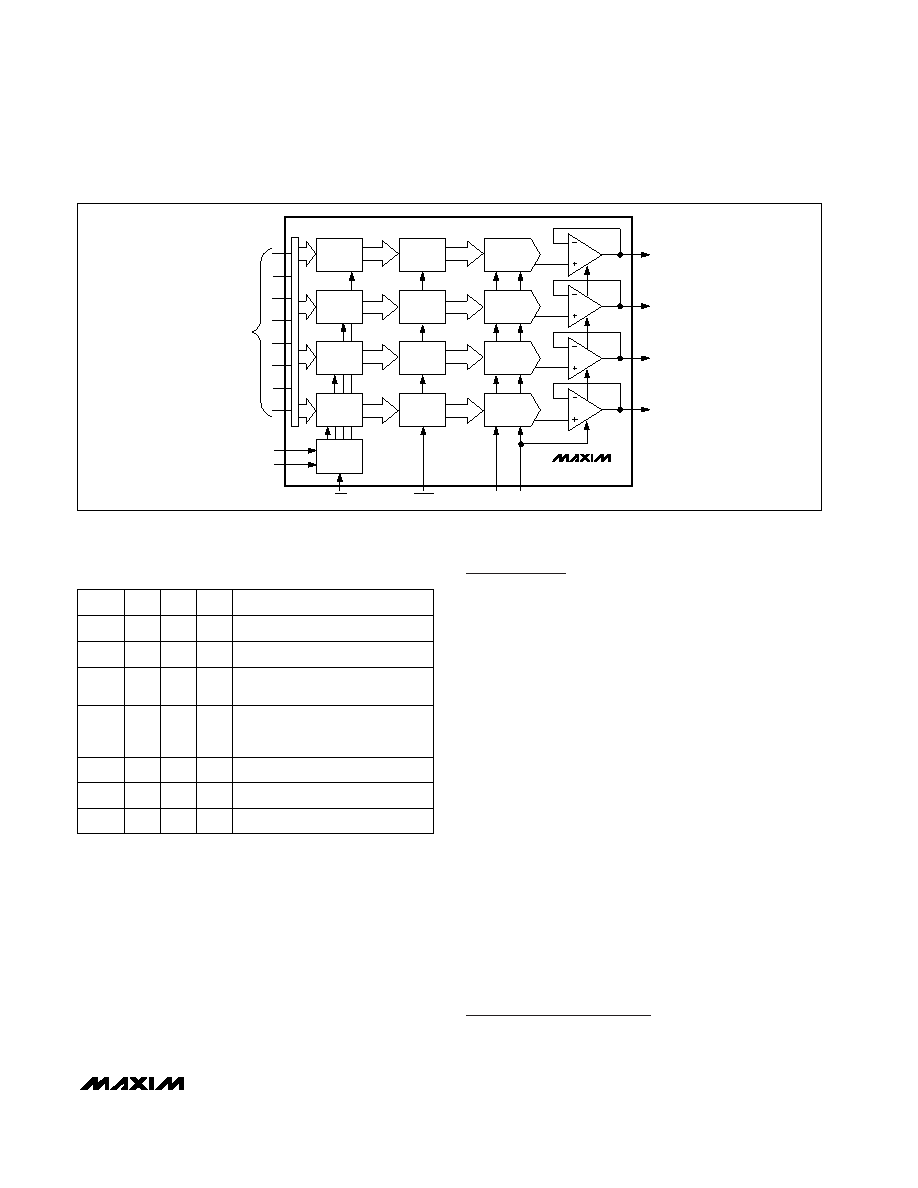
OUTC
OUTD
MAX5100
DAC C
DAC D
INPUT
LATCH C
DAC C
LATCH
INPUT
LATCH D
DAC D
LATCH
CONTROL
LOGIC
SHDN
REF
A1
AO
D0–D7
WR
LDAC
OUTA
OUTB
DAC A
DAC B
INPUT
LATCH A
DAC A
LATCH
INPUT
LATCH B
DAC B
LATCH
Figure 2. Functional Diagram
H = High state, L = Low state, X = Don’t care
Table 1. MAX5100 Address Table (Partial)
A0
X
L
X
L
H
L
H
A1
X
L
X
L
H
L
WR
LATCH STATE
H
Input and DAC data latched
H
L
DAC A input latch transparent
LDAC
L
H
All 4 DACs’ DAC latches
transparent
L
DAC A input registers transpar-
ent and all 4 DACs’ DAC
latches transparent
H
L
DAC D input latch transparent
H
L
DAC C input latch transparent
H
L
DAC B input latch transparent
相关PDF资料 |
PDF描述 |
|---|---|
| VI-BW1-IV-S | CONVERTER MOD DC/DC 12V 150W |
| LM2903NG | IC COMP DUAL OFFSET LV 8DIP |
| LM393AM | IC COMPARATOR DUAL DIFF 8-SOP |
| VE-2ND-CU-F1 | CONVERTER MOD DC/DC 85V 200W |
| LM393AN | IC COMPRTR DUAL 0-70DEG C 8-DIP |
相关代理商/技术参数 |
参数描述 |
|---|---|
| MAX5100AEUP+ | 功能描述:数模转换器- DAC 8-Bit 4Ch Precision DAC RoHS:否 制造商:Texas Instruments 转换器数量:1 DAC 输出端数量:1 转换速率:2 MSPs 分辨率:16 bit 接口类型:QSPI, SPI, Serial (3-Wire, Microwire) 稳定时间:1 us 最大工作温度:+ 85 C 安装风格:SMD/SMT 封装 / 箱体:SOIC-14 封装:Tube |
| MAX5100AEUP+T | 功能描述:数模转换器- DAC 8-Bit 4Ch Precision DAC RoHS:否 制造商:Texas Instruments 转换器数量:1 DAC 输出端数量:1 转换速率:2 MSPs 分辨率:16 bit 接口类型:QSPI, SPI, Serial (3-Wire, Microwire) 稳定时间:1 us 最大工作温度:+ 85 C 安装风格:SMD/SMT 封装 / 箱体:SOIC-14 封装:Tube |
| MAX5100AEUP-T | 功能描述:数模转换器- DAC RoHS:否 制造商:Texas Instruments 转换器数量:1 DAC 输出端数量:1 转换速率:2 MSPs 分辨率:16 bit 接口类型:QSPI, SPI, Serial (3-Wire, Microwire) 稳定时间:1 us 最大工作温度:+ 85 C 安装风格:SMD/SMT 封装 / 箱体:SOIC-14 封装:Tube |
| MAX5100BEUP | 功能描述:数模转换器- DAC RoHS:否 制造商:Texas Instruments 转换器数量:1 DAC 输出端数量:1 转换速率:2 MSPs 分辨率:16 bit 接口类型:QSPI, SPI, Serial (3-Wire, Microwire) 稳定时间:1 us 最大工作温度:+ 85 C 安装风格:SMD/SMT 封装 / 箱体:SOIC-14 封装:Tube |
| MAX5100BEUP+ | 功能描述:数模转换器- DAC 8-Bit 4Ch Precision DAC RoHS:否 制造商:Texas Instruments 转换器数量:1 DAC 输出端数量:1 转换速率:2 MSPs 分辨率:16 bit 接口类型:QSPI, SPI, Serial (3-Wire, Microwire) 稳定时间:1 us 最大工作温度:+ 85 C 安装风格:SMD/SMT 封装 / 箱体:SOIC-14 封装:Tube |
发布紧急采购,3分钟左右您将得到回复。