- 您现在的位置:买卖IC网 > PDF目录10769 > MAX5104EEE (Maxim Integrated Products)IC DAC DUAL 12BIT W/INTER 16QSOP PDF资料下载
参数资料
| 型号: | MAX5104EEE |
| 厂商: | Maxim Integrated Products |
| 文件页数: | 9/12页 |
| 文件大小: | 0K |
| 描述: | IC DAC DUAL 12BIT W/INTER 16QSOP |
| 产品培训模块: | Lead (SnPb) Finish for COTS Obsolescence Mitigation Program |
| 标准包装: | 100 |
| 设置时间: | 15µs |
| 位数: | 12 |
| 数据接口: | 串行 |
| 转换器数目: | 2 |
| 电压电源: | 单电源 |
| 工作温度: | -40°C ~ 85°C |
| 安装类型: | 表面贴装 |
| 封装/外壳: | 16-SSOP(0.154",3.90mm 宽) |
| 供应商设备封装: | 16-QSOP |
| 包装: | 管件 |
| 输出数目和类型: | 2 电压,单极;2 电压,双极 |
| 采样率(每秒): | * |
MAX5104
Low-Power, Dual, Voltage-Output, 12-Bit DAC
with Serial Interface
6
_______________________________________________________________________________________
_______________Detailed Description
The MAX5104 dual, 12-bit, voltage-output DAC is easily
configured with a 3-wire serial interface. The device
includes a 16-bit data-in/data-out shift register, and
each DAC has a double-buffered input composed of an
input register and a DAC register (see
Functional
Diagram). In addition, trimmed internal resistors produce
an internal gain of +2V/V that maximizes output voltage
swing. The amplifier’s offset-adjust pin allows for a DC
shift in the DAC’s output.
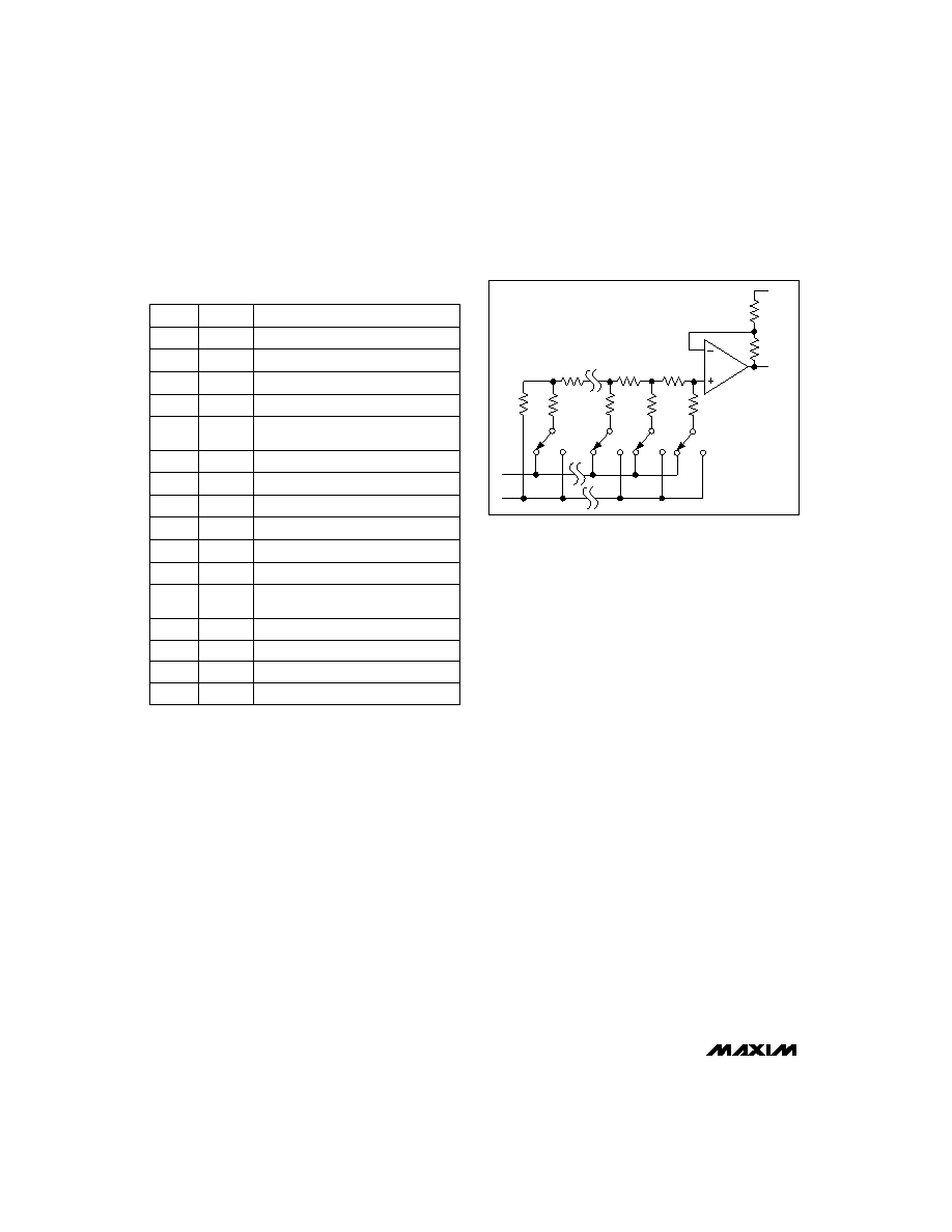
Both DACs use an inverted R-2R ladder network that
produces a weighted voltage proportional to the input
voltage value. Each DAC has its own reference input to
facilitate independent full-scale values. Figure 1 depicts
a simplified circuit diagram of one of the two DACs.
Reference Inputs
The reference inputs accept both AC and DC values
with a voltage range extending from 0 to (VDD - 1.4V).
Determine the output voltage using the following equa-
tion (OS_ = AGND):
VOUT = (VREF NB / 4096) 2
where NB is the numeric value of the DAC’s binary input
code (0 to 4095) and VREF is the reference voltage.
The reference input impedance ranges from 14k
(1554
hex) to several gigohms (with an input code of 0000
hex). The reference input capacitance is code depen-
dent and typically ranges from 15pF with an input code
of all zeros to 50pF with a full-scale input code.
Output Amplifier
The MAX5104’s output amplifiers have internal resistors
that provide for a gain of +2V/V when OS_ is connected
to AGND. These resistors are trimmed to minimize gain
error. The output amplifiers have a typical slew rate of
0.75V/s and settle to 1/2LSB within 15s, with a load
of 10k
in parallel with 100pF. Loads less than 2k
degrade performance.
The OS_ pin can be used to produce an adjustable off-
set voltage at the output. For instance, to achieve a 1V
offset, apply -1V to the OS_ pin to produce an output
range from 1V to (1V + VREF 2). Note that the DAC’s
output range is still limited by the maximum output voltage
specification.
Power-Down Mode
The MAX5104 features a software-programmable shut-
down mode that reduces the typical supply current to
2A. The two DACs can be powered down indepen-
dently, or simultaneously using the appropriate pro-
gramming command. Enter power-down mode by
writing the appropriate input-control word (Table 1). In
power-down mode, the reference inputs and amplifier
outputs become high impedance, and the serial inter-
face remains active. Data in the input registers is saved,
Digital Ground
DGND
9
Serial-Data Output
DOUT
10
User-Programmable Output
UPO
11
Power-Down Lockout. The device can-
not be powered down when
PDL is low.
PDL
12
Reference for DAC B
REFB
13
Active-Low Clear Input. Resets all reg-
isters to zero. DAC outputs go to 0V.
CL
5
Chip-Select Input
CS
6
Serial-Data Input
DIN
7
Serial-Clock Input
SCLK
8
Reference for DAC A
REFA
4
DAC A Offset Adjustment
OSA
3
PIN
DAC A Output Voltage
OUTA
2
Analog Ground
AGND
1
FUNCTION
NAME
14
OSB
DAC B Offset Adjustment
15
OUTB
DAC B Output Voltage
16
VDD
Positive Power Supply
OUT_
OS_
R
D0
D10
D11
D12
2R
RR
R
REF_
AGND
Figure 1. Simplified DAC Circuit Diagram
_____________________Pin Description
相关PDF资料 |
PDF描述 |
|---|---|
| LM393NG | IC COMP DUAL OFFSET LV 8DIP |
| MAX5102BEUE | IC DAC 8BIT DUAL PARALL 16-TSSOP |
| VE-2NF-CU-F4 | CONVERTER MOD DC/DC 72V 200W |
| B37931K9473K070 | CAP CER 0.047UF 16V 10% X7R 0603 |
| MAX5102AEUE | IC DAC 8BIT DUAL PARALL 16-TSSOP |
相关代理商/技术参数 |
参数描述 |
|---|---|
| MAX5104EEE+ | 功能描述:数模转换器- DAC 12-Bit 2Ch Precision DAC RoHS:否 制造商:Texas Instruments 转换器数量:1 DAC 输出端数量:1 转换速率:2 MSPs 分辨率:16 bit 接口类型:QSPI, SPI, Serial (3-Wire, Microwire) 稳定时间:1 us 最大工作温度:+ 85 C 安装风格:SMD/SMT 封装 / 箱体:SOIC-14 封装:Tube |
| MAX5104EEE+T | 功能描述:数模转换器- DAC 12-Bit 2Ch Precision DAC RoHS:否 制造商:Texas Instruments 转换器数量:1 DAC 输出端数量:1 转换速率:2 MSPs 分辨率:16 bit 接口类型:QSPI, SPI, Serial (3-Wire, Microwire) 稳定时间:1 us 最大工作温度:+ 85 C 安装风格:SMD/SMT 封装 / 箱体:SOIC-14 封装:Tube |
| MAX5104EEE-T | 功能描述:数模转换器- DAC RoHS:否 制造商:Texas Instruments 转换器数量:1 DAC 输出端数量:1 转换速率:2 MSPs 分辨率:16 bit 接口类型:QSPI, SPI, Serial (3-Wire, Microwire) 稳定时间:1 us 最大工作温度:+ 85 C 安装风格:SMD/SMT 封装 / 箱体:SOIC-14 封装:Tube |
| MAX5104XXXXX | 制造商:ZARLINK 制造商全称:Zarlink Semiconductor Inc 功能描述:RADIATION HARD 4096 x 1 BIT STATIC RAM |
| MAX5105 | 制造商:MAXIM 制造商全称:Maxim Integrated Products 功能描述:Nonvolatile, Quad, 8-Bit DACs |
发布紧急采购,3分钟左右您将得到回复。