- 您现在的位置:买卖IC网 > PDF目录3275 > MAX5166MECM+T (Maxim Integrated Products)IC AMP SAMPLE/HOLD 32CH 48-LQFP PDF资料下载
参数资料
| 型号: | MAX5166MECM+T |
| 厂商: | Maxim Integrated Products |
| 文件页数: | 5/12页 |
| 文件大小: | 0K |
| 描述: | IC AMP SAMPLE/HOLD 32CH 48-LQFP |
| 产品培训模块: | Lead (SnPb) Finish for COTS Obsolescence Mitigation Program |
| 标准包装: | 2,000 |
| 放大器类型: | 采样和保持 |
| 电路数: | 32 |
| 电流 - 输入偏压: | 1µA |
| 电压 - 输入偏移: | 5000µV |
| 电流 - 电源: | 36mA |
| 电流 - 输出 / 通道: | 2mA |
| 工作温度: | -40°C ~ 85°C |
| 安装类型: | 表面贴装 |
| 封装/外壳: | 48-LQFP |
| 供应商设备封装: | 48-LQFP(7x7) |
| 包装: | 带卷 (TR) |
MAX5166
32-Channel Sample/Hold Amplifier
with Four Multiplexed Inputs
2
_______________________________________________________________________________________
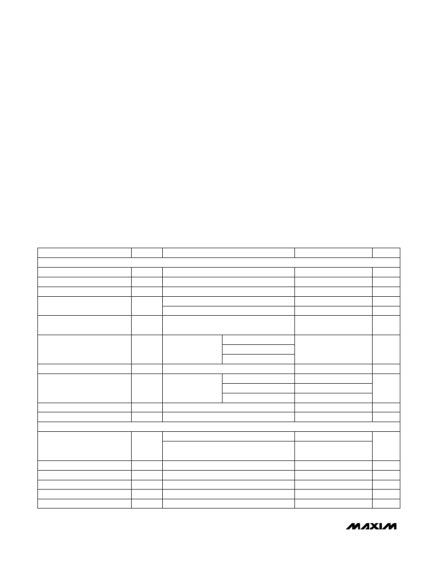
ABSOLUTE MAXIMUM RATINGS
ELECTRICAL CHARACTERISTICS
(VDD = +10V, VSS = -5V, VL = +5V ±5%, AGND = DGND, RL = 5k
, CL = 50pF, TA = TMIN to TMAX, unless otherwise noted. Typical
values are at TA = +25°C.)
Stresses beyond those listed under “Absolute Maximum Ratings” may cause permanent damage to the device. These are stress ratings only, and functional
operation of the device at these or any other conditions beyond those indicated in the operational sections of the specifications is not implied. Exposure to
absolute maximum rating conditions for extended periods may affect device reliability.
VDD to AGND.......................................................-0.3V to +11.0V
VSS to AGND .........................................................-6.0V to +0.3V
VDD to VSS ......................................................................+15.75V
VL to DGND ...........................................................-0.3V to +6.0V
VL to AGND ...........................................................-0.3V to +6.0V
DGND to AGND.....................................................-0.3V to +2.0V
IN_ to AGND ...............................................................VSS to VDD
A_, M_ to DGND ....................................................-0.3V to +6.0V
Maximum Current into Output Pin ....................................±10mA
Maximum Current into A_, M_ ..........................................±20mA
Continuous Power Dissipation (TA = +70°C)
48-Pin TQFP (derate 12.5mW/°C above +70°C)..................1W
Operating Temperature Ranges
MAX5166_CCM ...................................................0°C to +70°C
MAX5166_ECM.................................................-40°C to +85°C
Storage Temperature Range .............................-65°C to +150°C
Lead Temperature (soldering, 10sec) .............................+300°C
Figure 2 (Note 1)
IN_ = AGND
To ±1mV of final value, Figure 2 (Note 1)
-4V < VIN < +7V, RL =
∞
TA = +25°C, 100mV step to ±1mV, RL =
∞,
Figure 2 (Note 2)
8V step to 0.08%, RL =
∞, Figure 2 (Note 2)
(Note 1)
IN_ = AGND, TA = +25°C
+15°C
≤ TA ≤ +65°C (Note 1)
RL =
∞,
CL = 250pF
CONDITIONS
ns
150
tDH
Data Hold Time
ns
200
tPW
Inhibit Pulse Width
ns
200
tAP
Aperture Delay
s
12
tH
Hold-Mode Settling Time
s
1
tAQ
2.5
4
Acquisition Time
mA
2
ISINK
Output Sink Current
mA
2
ISOURCE
Output Source Current
700
1000
1300
ROUT_
DC Output Impedance
mV
0.25
1.00
VHS
Hold Step
%
0.01
0.08
Linearity Error
350
500
650
35
50
65
pF
520
CIN_
Input Capacitance
mV/sec
140
VOUT
Droop Rate
mV
-30
-5
+30
V/°C
20
40
VOS
Offset Voltage
UNITS
MIN
TYP
MAX
SYMBOL
PARAMETER
8V step with
500ns rising edge
(Note 1)
Analog Crosstalk
MAX5166L
MAX5166M
MAX5166N
RL =
∞
V
VSS +
VDD -
0.75
2.4
VOUT_
Output Voltage Range
MAX5165M, CL = 10nF
MAX5165N, CL = 10nF
MAX5165L, CL = 250pF
Figure 2 (Note 1)
ns
50
tDS
Data Setup Time
ANALOG SECTION
TIMING PERFORMANCE
dB
-72
-76
相关PDF资料 |
PDF描述 |
|---|---|
| RMCF0402JT68R0 | RES TF 68 OHM 5% 1/16W 0402 |
| RP93737T0050GTTR | RES TERM 50 OHM 40W 2GHZ |
| MAX5167NCCM+T | IC AMP SAMPLE/HOLD 32CH 48-LQFP |
| RP43737R0100GTTR | RES 100 OHM 2% 40W SMD |
| RP93725T0050GTTR | RES TERM 50 OHM 30W 2GHZ |
相关代理商/技术参数 |
参数描述 |
|---|---|
| MAX5166NCCM | 功能描述:采样&保持放大器 RoHS:否 制造商:Texas Instruments 通道数量:2 捕获时间:20 us 电源电压-最大:18 V 最大工作温度:+ 85 C 最小工作温度:- 25 C 安装风格: 封装 / 箱体:SOIC-14 封装:Tube |
| MAX5166NCCM+ | 功能描述:采样&保持放大器 32Ch Sample/Hold Amp RoHS:否 制造商:Texas Instruments 通道数量:2 捕获时间:20 us 电源电压-最大:18 V 最大工作温度:+ 85 C 最小工作温度:- 25 C 安装风格: 封装 / 箱体:SOIC-14 封装:Tube |
| MAX5166NCCM+T | 功能描述:采样&保持放大器 32Ch Sample/Hold Amp RoHS:否 制造商:Texas Instruments 通道数量:2 捕获时间:20 us 电源电压-最大:18 V 最大工作温度:+ 85 C 最小工作温度:- 25 C 安装风格: 封装 / 箱体:SOIC-14 封装:Tube |
| MAX5166NCCM-T | 功能描述:采样&保持放大器 RoHS:否 制造商:Texas Instruments 通道数量:2 捕获时间:20 us 电源电压-最大:18 V 最大工作温度:+ 85 C 最小工作温度:- 25 C 安装风格: 封装 / 箱体:SOIC-14 封装:Tube |
| MAX5166NECM | 功能描述:采样&保持放大器 RoHS:否 制造商:Texas Instruments 通道数量:2 捕获时间:20 us 电源电压-最大:18 V 最大工作温度:+ 85 C 最小工作温度:- 25 C 安装风格: 封装 / 箱体:SOIC-14 封装:Tube |
发布紧急采购,3分钟左右您将得到回复。