- 您现在的位置:买卖IC网 > PDF目录2010 > MAX522EPA+ (Maxim Integrated Products)IC DAC 8BIT DUAL SERIAL 8-DIP PDF资料下载
参数资料
| 型号: | MAX522EPA+ |
| 厂商: | Maxim Integrated Products |
| 文件页数: | 10/12页 |
| 文件大小: | 0K |
| 描述: | IC DAC 8BIT DUAL SERIAL 8-DIP |
| 产品培训模块: | Lead (SnPb) Finish for COTS Obsolescence Mitigation Program |
| 标准包装: | 50 |
| 设置时间: | 70µs |
| 位数: | 8 |
| 数据接口: | 串行 |
| 转换器数目: | 2 |
| 电压电源: | 单电源 |
| 工作温度: | -40°C ~ 85°C |
| 安装类型: | 通孔 |
| 封装/外壳: | 8-DIP(0.300",7.62mm) |
| 供应商设备封装: | 8-PDIP |
| 包装: | 管件 |
| 输出数目和类型: | 2 电压,单极 |
| 采样率(每秒): | * |
MAX522
Dual, 8-Bit, Voltage-Output
Serial DAC in 8-Pin SO Package
_______________________________________________________________________________________
7
_______________Detailed Description
Analog Section
The MAX522 contains two 8-bit, voltage-output digital-
to-analog converters (DACs). The DACs are “inverted”
R-2R ladder networks using complementary switches
that convert 8-bit digital inputs into equivalent analog
output voltages in proportion to the applied reference
voltage.
The MAX522 has one reference input which is shared
by DAC A and DAC B. The device includes output
buffer amplifiers for both DACs and input logic for sim-
ple microprocessor (P) and CMOS interfaces. The
power-supply range is from +5.5V down to +2.7V.
Reference Input and DAC Output Range
The voltage at REF sets the full-scale output of the
DACs. The input impedance of the REF input is code
dependent. The lowest value, approximately 8k
,
occurs when the input code is 01010101 (55hex). The
maximum value of infinity occurs when the input code
is zero.
In shutdown mode, the selected DAC output is set to
zero while the value stored in the DAC register remains
unchanged. This removes the load from the reference
input to save power. Bringing the MAX522 out of shut-
down mode restores the DAC output voltage. Because
the input resistance at REF is code dependent, the
DAC’s reference sources should have an output
impedance of no more than 5
. The input capacitance
at the REF pin is also code dependent and typically
does not exceed 25pF.
The reference voltage on REF can range anywhere from
GND to VDD. See the Output Buffer Amplifier section for
more information.
Output Buffer Amplifiers
DAC A and DAC B voltage outputs are internally
buffered. The buffer amplifiers have a rail-to-rail
(GND to VDD) output voltage range.
The DAC outputs are internally divided by two and the
buffer is set to a gain of two, eliminating the need for a
buffer input voltage range to the positive supply rail.
DAC A’s output amplifier can source and sink up to
5mA of current (0.5mA for DAC B’s buffer). See the
Total Unadjusted Error vs. Digital Code graph in the
Typical Operating Characteristics. The amplifier is
unity-gain stable with a capacitive load of 0.1F
(0.01F for DAC B’s buffer) or greater. The slew rate is
limited by the load capacitor and is typically 0.1V/s
with a 0.1F load (0.01F for DAC B’s buffer).
Shutdown Mode
When programmed to shutdown mode, the outputs of
DAC A and DAC B go into a high-impedance state.
Virtually no current flows into or out of the buffer ampli-
fiers in that state. In shutdown mode, the REF inputs
are high impedance (2M
typical) to conserve current
drain from the system reference; therefore, the system
reference does not have to be powered down.
Coming out of shutdown, the DAC outputs return to the
values kept in the registers. The recovery time is equiv-
alent to the DAC settling time.
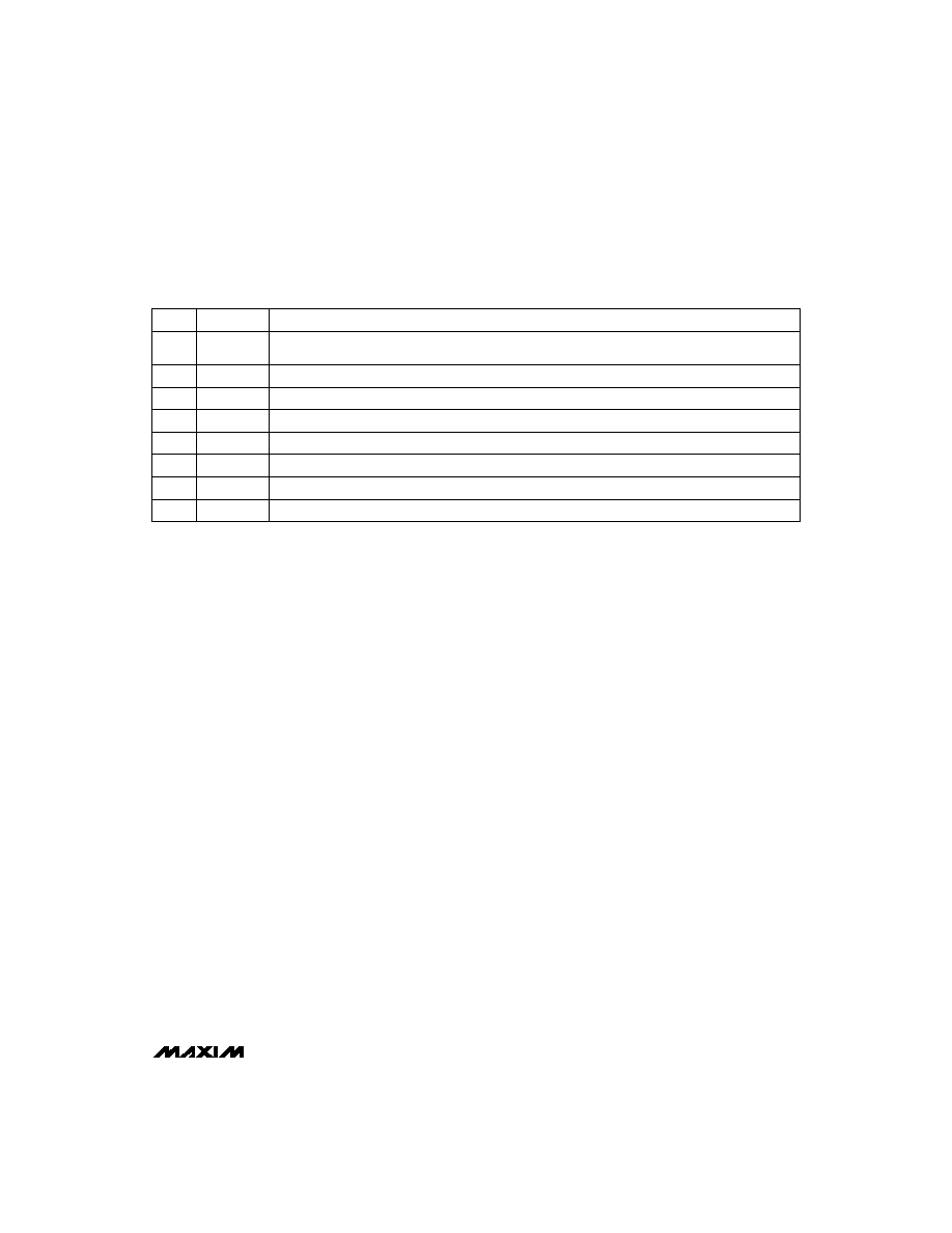
______________________________________________________________Pin Description
NAME
FUNCTION
1
–
C
—
S
–
Chip Select (active low). Enables data to be shifted into the 16-bit shift register. Programming commands
are executed at the rising edge of
–
C
—
S
–
.
2
SCLK
Serial Clock Input. Data is clocked in on the rising edge of SCLK.
PIN
3
VDD
Positive Power Supply (2.7V to 5.5V). Bypass with 0.22F to GND.
4
GND
Ground
8
DIN
Serial Data Input of the 16-bit shift register. Data is clocked into the register on the rising edge of SCLK.
7
REF
Reference Input for DAC A and DAC B
6
OUTB
DAC B Output Voltage (Buffered). Connect 0.01F capacitor or greater to GND.
5
OUTA
DAC A Output Voltage (Buffered). Connect 0.1F capacitor or greater to GND.
相关PDF资料 |
PDF描述 |
|---|---|
| MAX5233EEE+ | IC DAC 10BIT DUAL 5V SER 16-QSOP |
| MAX5237EUB+ | IC DAC 10BIT DUAL 5V 10-UMAX |
| MAX5253AEAP+ | IC DAC 12BIT QUAD 3V 20-SSOP |
| MAX5258EEE+T | IC DAC 8BIT OCTAL 5V 16-QSOP |
| MAX525AEAP+ | IC DAC 12BIT QUAD LP 20-SSOP |
相关代理商/技术参数 |
参数描述 |
|---|---|
| MAX522EPA+ | 功能描述:数模转换器- DAC 8-Bit 2Ch Precision DAC RoHS:否 制造商:Texas Instruments 转换器数量:1 DAC 输出端数量:1 转换速率:2 MSPs 分辨率:16 bit 接口类型:QSPI, SPI, Serial (3-Wire, Microwire) 稳定时间:1 us 最大工作温度:+ 85 C 安装风格:SMD/SMT 封装 / 箱体:SOIC-14 封装:Tube |
| MAX522ESA | 功能描述:数模转换器- DAC RoHS:否 制造商:Texas Instruments 转换器数量:1 DAC 输出端数量:1 转换速率:2 MSPs 分辨率:16 bit 接口类型:QSPI, SPI, Serial (3-Wire, Microwire) 稳定时间:1 us 最大工作温度:+ 85 C 安装风格:SMD/SMT 封装 / 箱体:SOIC-14 封装:Tube |
| MAX522ESA+ | 功能描述:数模转换器- DAC 8-Bit 2Ch Precision DAC RoHS:否 制造商:Texas Instruments 转换器数量:1 DAC 输出端数量:1 转换速率:2 MSPs 分辨率:16 bit 接口类型:QSPI, SPI, Serial (3-Wire, Microwire) 稳定时间:1 us 最大工作温度:+ 85 C 安装风格:SMD/SMT 封装 / 箱体:SOIC-14 封装:Tube |
| MAX522ESA+T | 功能描述:数模转换器- DAC 8-Bit 2Ch Precision DAC RoHS:否 制造商:Texas Instruments 转换器数量:1 DAC 输出端数量:1 转换速率:2 MSPs 分辨率:16 bit 接口类型:QSPI, SPI, Serial (3-Wire, Microwire) 稳定时间:1 us 最大工作温度:+ 85 C 安装风格:SMD/SMT 封装 / 箱体:SOIC-14 封装:Tube |
| MAX522ESA-T | 功能描述:数模转换器- DAC RoHS:否 制造商:Texas Instruments 转换器数量:1 DAC 输出端数量:1 转换速率:2 MSPs 分辨率:16 bit 接口类型:QSPI, SPI, Serial (3-Wire, Microwire) 稳定时间:1 us 最大工作温度:+ 85 C 安装风格:SMD/SMT 封装 / 箱体:SOIC-14 封装:Tube |
发布紧急采购,3分钟左右您将得到回复。