- 您现在的位置:买卖IC网 > PDF目录385533 > MAX530 (Maxim Integrated Products, Inc.) +5V, Low-Power, Parallel-Input, Voltage-Output, 12-Bit DAC(单通道,电压输出,12位并行D/A转换器) PDF资料下载
参数资料
| 型号: | MAX530 |
| 厂商: | Maxim Integrated Products, Inc. |
| 英文描述: | +5V, Low-Power, Parallel-Input, Voltage-Output, 12-Bit DAC(单通道,电压输出,12位并行D/A转换器) |
| 中文描述: | +5V、低功耗、并行输入、电压输出、12位DAC |
| 文件页数: | 9/16页 |
| 文件大小: | 179K |
| 代理商: | MAX530 |
Output Buffer
The output amplifier uses a folded cascode input stage
and a type AB output stage. Large output devices with
low series resistance allow the output to swing to
ground in single-supply operation. The output buffer is
unity-gain stable. Input offset voltage and supply cur-
rent are laser trimmed. Settling time is 25μs to 0.01% of
final value. The output is short-circuit protected and
can drive a 2k
load with more than 100pF of load
capacitance. The op amp may be placed in unity-gain
(G = 1), in a gain of two (G = 2), or in a bipolar-output
mode by using the ROFS and RFB pins. These pins are
used to define a DAC output voltage range of 0V to
+2.048V, 0V to +4.096V or ±2.048V, by connecting
ROFS to VOUT, GND, or REFIN. RFB is always con-
nected to VOUT. Table 1 summarizes ROFS usage.
External Referenc e
An external reference in the range (V
SS
+ 2V) to
(V
DD
- 2V) may be used with the MAX530 in dual-sup-
ply, unity-gain operation. In single-supply, unity-gain
operation, the reference must be positive and may not
exceed (V
DD
- 2V). The reference voltage determines
the DAC’s full-scale output. Because of the code-
dependent nature of reference input impedances, a
high-quality, low-output-impedance amplifier (such as
the MAX480 low-power, precision op amp) should be
used to drive REFIN.
If an upgrade to the internal reference is required, the
2.5V MAX873A is ideal: ±15mV initial accuracy,
7ppm/°C (max) temperature coefficient.
Power-On Reset
An internal power-on reset (POR) circuit forces the
DAC register to reset to all 0s when V
DD
is first applied.
The POR pulse is typically 1.3μs; however, it may take
2ms for the internal reference to charge its large filter
capacitor and settle to its trimmed value.
In addition to POR , a clear (CLR) pin, when held low,
sets the DAC register to all 0s. CLR operates asynchro-
nously and independently from chip select (CS). With
the DAC input at all 0s, the op-amp output is at zero for
unity-gain and G = 2 configurations, but it is at -V
REF
for the bipolar configuration.
S hutdown Mode
The MAX530 is designed for low power consumption.
Understanding the circuit allows power consumption
management for maximum efficiency. In single-supply
mode (V
DD
= +5V, V
SS
= GND) the initial supply cur-
rent is typically only 160μA, including the reference, op
amp, and DAC. This low current occurs when the
power-on reset circuit clears the DAC to all 0s and
forces the op-amp output to zero (unipolar mode only).
See the Supply Current vs. REFIN graph in the Typical
Operating Characteristics. Under this condition, there
is no internal load on the reference (DAC = 000hex,
REFIN is open circuit) and the op amp operates at its
minimum quiescent current. The CLR signal resets the
MAX530 to these same conditions and can be used to
control a power-saving mode when the DAC is not
being used by the system.
M
+5V, Low-Power, Parallel-Input,
Voltage-Output, 12-Bit DAC
_______________________________________________________________________________________
9
ROFS
CONNECTED TO:
DAC OUTPUT
RANGE
OP-AMP
GAIN
VOUT
0V to 2.048V
G = 1
AGND
0V to 4.096V
G = 2
REFIN
-2.048V to +2.048V
Bipolar
Note:
Assumes RFB = VOUT and REFIN = REFOUT = 2.048V
Table 1. ROFS Usage
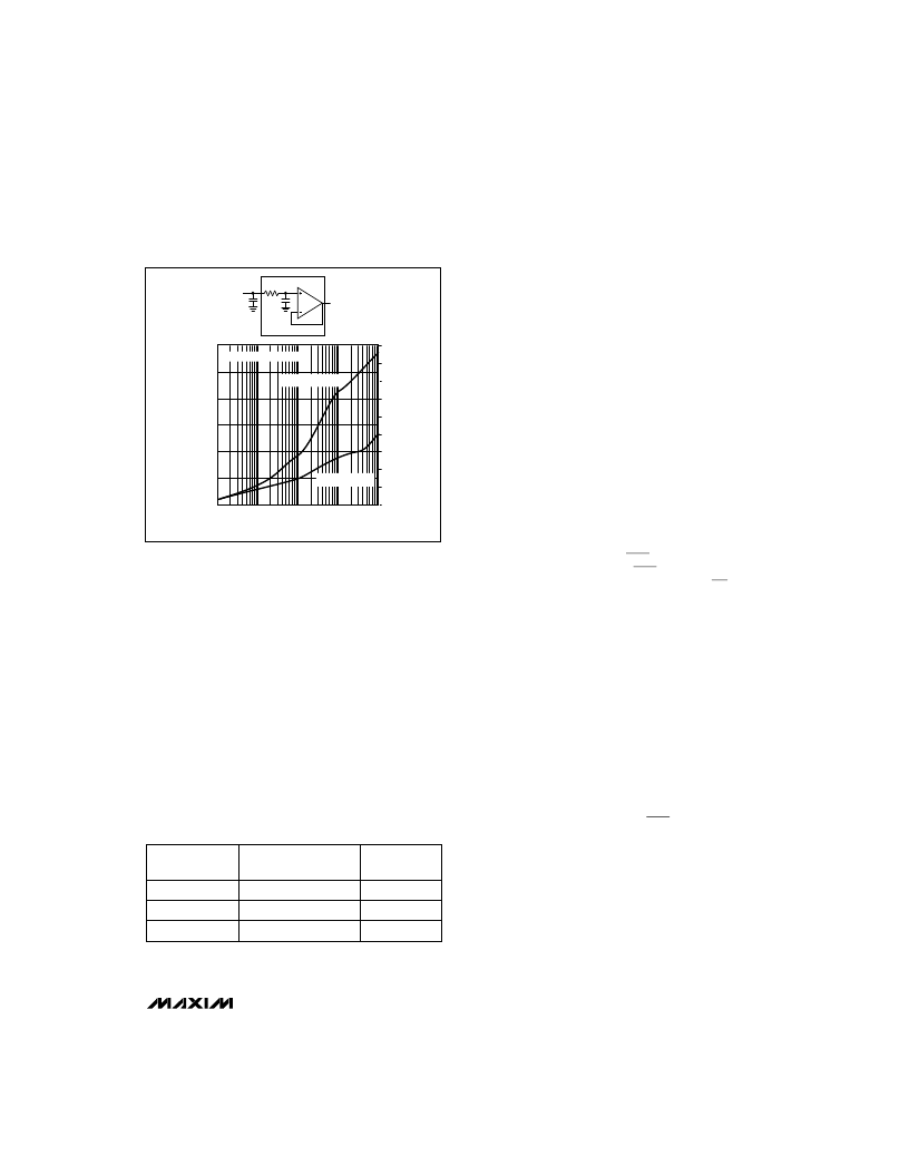
Figure 2. Reference Noise vs. Frequency
300
50
1
10
100
100
M
FREQUENCY (kHz)
R
R
)
150
200
250
0
0.1
1000
TOTAL
REFERERNCE
NOISE
R
S
REFOUT
C
REFOUT
C
S
TEK 7A22
C
REFOUT
= 3.3
μ
F
C
REFOUT
= 47
μ
F
SINGLE POLE ROLLOFF
1.8
1.6
1.4
1.2
1.0
0.8
0.6
0.4
0.2
0.0
R
相关PDF资料 |
PDF描述 |
|---|---|
| MAX5312EAE | +-10V, 12-Bit, Serial, Voltage-Output DAC |
| MAX531 | +5V, Low-Power, Voltage-Output, Serial 12-Bit DACs(单通道,电压输出,12位串行D/A转换器) |
| MAX538 | +5V, Low-Power, Voltage-Output, Serial 12-Bit DACs(单通道,电压输出,12位串行D/A转换器) |
| MAX532 | Dual, Serial-Input, Voltage-Output, 12-Bit MDAC(双通道,串行输入,电压输出,12位D/A转换器) |
| MAX5363 | Low-Cost, Low-Power, 6-Bit DACs with 3-Wire Serial Interface in SOT23 |
相关代理商/技术参数 |
参数描述 |
|---|---|
| MAX5302CUA | 功能描述:数模转换器- DAC RoHS:否 制造商:Texas Instruments 转换器数量:1 DAC 输出端数量:1 转换速率:2 MSPs 分辨率:16 bit 接口类型:QSPI, SPI, Serial (3-Wire, Microwire) 稳定时间:1 us 最大工作温度:+ 85 C 安装风格:SMD/SMT 封装 / 箱体:SOIC-14 封装:Tube |
| MAX5302CUA+ | 功能描述:数模转换器- DAC 12-Bit Precision DAC RoHS:否 制造商:Texas Instruments 转换器数量:1 DAC 输出端数量:1 转换速率:2 MSPs 分辨率:16 bit 接口类型:QSPI, SPI, Serial (3-Wire, Microwire) 稳定时间:1 us 最大工作温度:+ 85 C 安装风格:SMD/SMT 封装 / 箱体:SOIC-14 封装:Tube |
| MAX5302CUA+T | 功能描述:数模转换器- DAC 12-Bit Precision DAC RoHS:否 制造商:Texas Instruments 转换器数量:1 DAC 输出端数量:1 转换速率:2 MSPs 分辨率:16 bit 接口类型:QSPI, SPI, Serial (3-Wire, Microwire) 稳定时间:1 us 最大工作温度:+ 85 C 安装风格:SMD/SMT 封装 / 箱体:SOIC-14 封装:Tube |
| MAX5302CUA-T | 功能描述:数模转换器- DAC RoHS:否 制造商:Texas Instruments 转换器数量:1 DAC 输出端数量:1 转换速率:2 MSPs 分辨率:16 bit 接口类型:QSPI, SPI, Serial (3-Wire, Microwire) 稳定时间:1 us 最大工作温度:+ 85 C 安装风格:SMD/SMT 封装 / 箱体:SOIC-14 封装:Tube |
| MAX5302EUA | 功能描述:数模转换器- DAC RoHS:否 制造商:Texas Instruments 转换器数量:1 DAC 输出端数量:1 转换速率:2 MSPs 分辨率:16 bit 接口类型:QSPI, SPI, Serial (3-Wire, Microwire) 稳定时间:1 us 最大工作温度:+ 85 C 安装风格:SMD/SMT 封装 / 箱体:SOIC-14 封装:Tube |
发布紧急采购,3分钟左右您将得到回复。