- 您现在的位置:买卖IC网 > PDF目录2010 > MAX5312EAE+T (Maxim Integrated Products)IC DAC 12BIT 5V/10V SER 16-SSOP PDF资料下载
参数资料
| 型号: | MAX5312EAE+T |
| 厂商: | Maxim Integrated Products |
| 文件页数: | 8/19页 |
| 文件大小: | 0K |
| 描述: | IC DAC 12BIT 5V/10V SER 16-SSOP |
| 产品培训模块: | Lead (SnPb) Finish for COTS Obsolescence Mitigation Program |
| 标准包装: | 2,000 |
| 设置时间: | 10µs |
| 位数: | 12 |
| 数据接口: | 串行 |
| 转换器数目: | 1 |
| 电压电源: | 双 ± |
| 工作温度: | -40°C ~ 85°C |
| 安装类型: | 表面贴装 |
| 封装/外壳: | 16-SSOP(0.209",5.30mm 宽) |
| 供应商设备封装: | 16-SSOP |
| 包装: | 带卷 (TR) |
| 输出数目和类型: | 1 电压,单极;1 电压,双极 |
| 采样率(每秒): | * |

MAX5312
±10V, 12-Bit, Serial, Voltage-Output DAC
16
______________________________________________________________________________________
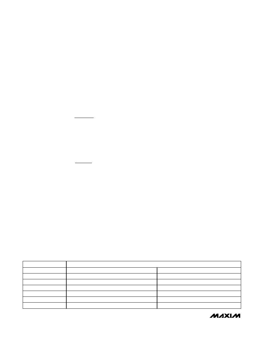
External Reference and Transfer
Functions
Connect an external 2V to 5.25V reference to REF (the
MAX6350 is recommended). Set the output voltage
range with the reference and the input code by using
the equations below.
Unipolar Output Voltage:
where
Bipolar Output Voltage:
where
where VOUT_UNI is the unipolar output voltage, VOUT_BIP
is the bipolar output voltage, LSBUNI is the unipolar LSB
step size, LSBBIP is the bipolar LSB step size, VREF is
the reference voltage, and CODE is the decimal equiva-
lent of the binary, 12-bit, DAC input code.
In either case, a 000hex input code produces the mini-
mum output (-2 x VREF for bipolar and 0 for unipolar),
an 800hex input code produces the midscale output (0
for bipolar and VREF for unipolar), and a FFFhex input
code produces the full-scale output (2 x VREF for bipo-
lar and unipolar).
Output Amplifiers
The output-amplifier section can be configured as
either unipolar or bipolar by the UNI/BIP logic input.
With UNI/BIP forced low, SW1 and SW2 in Figure 4 are
closed, and SW3 is open. This configuration channels
the DAC output through two output stages to generate
the ±2 x VREF output swing. The first amplifier gener-
ates the ±VREF voltage range and the second amplifier
increases it by two. When configured for bipolar opera-
tion, the MAX5312 must be driven with dual ±12V to
±15V power supplies.
With UNI/BIP forced high, switches SW1 and SW2 are
open, and SW3 is closed. This configuration channels
the DAC output through only a single gain stage to gen-
erate a 0 to (2 x VREF) output swing.
Daisy Chaining
SPI-/QSPI-/MICROWIRE-compatible devices can be
daisy chained to reduce I/O lines from the host con-
troller (Figure 7). Daisy chain devices by connecting
the DOUT of one device to the DIN of the next, and
connect the SCLK of all devices to a common clock.
Data is shifted out of DOUT 16.5 clock cycles after it is
shifted into DIN, and is available on the rising edge of
the 17th clock cycle. The SPI-/QSPI-/MICROWIRE-com-
patible serial interface normally works at up to 10MHz,
but must be slowed to 6.0MHz if daisy chaining. DOUT
is high impedance when CS is high.
Shutdown
Shutdown is controlled by software commands or by the
SHDN logic input. The SHDN logic input can be imple-
mented at any time. The SPI-/QSPI-/MICROWIRE-compat-
ible serial interface remains fully functional, and the device
is programmable while shut down. When shut down, the
MAX5312 supply current reduces to 3.5A, DOUT is high
impedance, and OUT is pulled to SGND through the inter-
nal feedback resistors of the output amplifier (Figure 1).
When coming out of shutdown, or during device power-
up, allow 350s for the output to stabilize.
LSB
V
BIP
REF
=
×
4
2
12
V
LSB
CODE
V
OUT BIP
BIP
REF
_
(
) (
)
=×
×
2
LSB
V
UNI
REF
= ×
2
12
V
LSB
CODE
OUT UNI
UNI
_
=×
BINARY DAC CODE
ANALOG OUTPUT
MSB
LSB
UNIPOLAR (UNI/
BIP_ = HIGH)
BIPOLAR (UNI/
BIP_ = LOW)
1111 1111 1111
+2 x VREF (4095 / 4096)
+2 x VREF (2047 / 2048)
1000 0000 0001
+2 x VREF (2049 / 4096)
+2 x VREF (1 / 2048)
1000 0000 0000
+2 x VREF (2048 / 4096) = VREF
0
0111 1111 1111
+2 x VREF (2047 / 4096)
-2 x VREF (1 / 2048)
0000 0000 0001
+2 x VREF (1 / 4096)
-2 x VREF (2047 / 2048)
0000 0000 0000
0
-2 x VREF (2048 / 2048) = -2 x VREF
Table 3. Output Voltage as Input Code Examples
相关PDF资料 |
PDF描述 |
|---|---|
| MAX5316GTG+ | IC DAC 16BIT SPI 24TQFN |
| MAX5322EAI+ | IC DAC 12BIT DUAL 10V SER 28SSOP |
| MAX532AEPE+ | IC MDAC 12BIT DUAL SER 16-DIP |
| MAX5355EUA+ | IC DAC 10BIT 3.3V VOLT OUT 8UMAX |
| MAX5362PEUK+T | IC DAC 6BIT LP 2WIRE SER SOT23-5 |
相关代理商/技术参数 |
参数描述 |
|---|---|
| MAX5312EVKIT+ | 功能描述:数据转换 IC 开发工具 MAX5312 Eval Kit RoHS:否 制造商:Texas Instruments 产品:Demonstration Kits 类型:ADC 工具用于评估:ADS130E08 接口类型:SPI 工作电源电压:- 6 V to + 6 V |
| MAX5316GTG+ | 功能描述:数模转换器- DAC 16-bit V Out SPI DAC w/Digi Gain & Offset RoHS:否 制造商:Texas Instruments 转换器数量:1 DAC 输出端数量:1 转换速率:2 MSPs 分辨率:16 bit 接口类型:QSPI, SPI, Serial (3-Wire, Microwire) 稳定时间:1 us 最大工作温度:+ 85 C 安装风格:SMD/SMT 封装 / 箱体:SOIC-14 封装:Tube |
| MAX5316GTG+T | 功能描述:数模转换器- DAC 16-bit V Out SPI DAC w/Digi Gain & Offset RoHS:否 制造商:Texas Instruments 转换器数量:1 DAC 输出端数量:1 转换速率:2 MSPs 分辨率:16 bit 接口类型:QSPI, SPI, Serial (3-Wire, Microwire) 稳定时间:1 us 最大工作温度:+ 85 C 安装风格:SMD/SMT 封装 / 箱体:SOIC-14 封装:Tube |
| MAX5317GTG+ | 功能描述:数模转换器- DAC 16Bit DAC w/Digital Gain/Offset Control RoHS:否 制造商:Texas Instruments 转换器数量:1 DAC 输出端数量:1 转换速率:2 MSPs 分辨率:16 bit 接口类型:QSPI, SPI, Serial (3-Wire, Microwire) 稳定时间:1 us 最大工作温度:+ 85 C 安装风格:SMD/SMT 封装 / 箱体:SOIC-14 封装:Tube |
| MAX5317GTG+T | 功能描述:数模转换器- DAC 16Bit DAC w/Digital Gain/Offset Control RoHS:否 制造商:Texas Instruments 转换器数量:1 DAC 输出端数量:1 转换速率:2 MSPs 分辨率:16 bit 接口类型:QSPI, SPI, Serial (3-Wire, Microwire) 稳定时间:1 us 最大工作温度:+ 85 C 安装风格:SMD/SMT 封装 / 箱体:SOIC-14 封装:Tube |
发布紧急采购,3分钟左右您将得到回复。