- 您现在的位置:买卖IC网 > PDF目录8923 > MAX536BCWE+ (Maxim Integrated Products)IC DAC QUAD CALBRTD 12BIT 16SOIC PDF资料下载
参数资料
| 型号: | MAX536BCWE+ |
| 厂商: | Maxim Integrated Products |
| 文件页数: | 7/24页 |
| 文件大小: | 0K |
| 描述: | IC DAC QUAD CALBRTD 12BIT 16SOIC |
| 产品培训模块: | Lead (SnPb) Finish for COTS Obsolescence Mitigation Program |
| 标准包装: | 46 |
| 设置时间: | 3µs |
| 位数: | 12 |
| 数据接口: | 串行 |
| 转换器数目: | 4 |
| 电压电源: | 双 ± |
| 功率耗散(最大): | 762mW |
| 工作温度: | 0°C ~ 70°C |
| 安装类型: | 表面贴装 |
| 封装/外壳: | 16-SOIC(0.295",7.50mm 宽) |
| 供应商设备封装: | 16-SOIC W |
| 包装: | 管件 |
| 输出数目和类型: | 4 电压,单极;4 电压,双极 |
| 采样率(每秒): | * |
| 产品目录页面: | 1394 (CN2011-ZH PDF) |
4), the DAC registers remain transparent. Any time an
input register is updated, the change appears at the DAC
output with the rising edge of CS.
The 4-wire interface (CS, SCK, SDI, LDAC) is similar to
the 3-wire interface with LDAC tied high, except LDAC is
a hardware input that simultaneously and asynchronously
loads all DAC registers from their respective input regis-
ters when driven low (Figure 5).
Serial-Interface Description
The MAX536/MAX537 require 16 bits of serial data. Data is
sent MSB first and can be sent in two 8-bit packets or one
16-bit word (CS must remain low until 16 bits are trans-
ferred). The serial data is composed of two DAC address
bits (A1, A0), two control bits (C1, C0), and the 12 data bits
D11…D0 (Figure 7). The 4-bit address/control code deter-
mines the following: 1) the register(s) to be updated and/or
the status of the input and DAC registers (i.e., whether they
are in transparent or latch mode), and 2) the edge on which
data is clocked out of SDO.
Figure 6 shows the serial-interface timing requirements. The
chip-select pin (CS) must be low to enable the DAC’s serial
interface. When CS is high, the interface control circuitry is
disabled and the serial data output pin (SDO) is driven high
(MAX537) or is a high-impedance open drain (MAX536). CS
must go low at least tCSS before the rising serial clock (SCK)
edge to properly clock in the first bit. When CS is low, data is
clocked into the internal shift register via the serial data input
pin (SDI) on SCK’s rising edge. The maximum guaranteed
clock frequency is 10MHz. Data is latched into the appropri-
ate MAX536/MAX537 input/DAC registers on CS’s rising
edge.
Interface timing is optimized when serial data is clocked out
of the microcontroller/microprocessor on one clock edge
and clocked into the MAX536/MAX537 on the other edge.
Table 1 lists the serial-interface programming commands.
For certain commands, the 12 data bits are “don’t cares”.
The programming command Load-All-DACs-From-Shift-
Register allows all input and DAC registers to be simultane-
ously loaded with the same digital code from the input shift
register. The NOP (no operation) command allows the regis-
ter contents to be unaffected and is useful when the
MAX536/MAX537 are configured in a daisy-chain (see the
Daisy-Chaining Devices section). The command to change
the clock edge on which serial data is shifted out of the
MAX536/MAX537 SDO pin also loads data from all input reg-
isters to their respective DAC registers.
Serial-Data Output
The serial-data output, SDO, is the internal shift register’s
output. The MAX536/MAX537 can be programmed so that
data is clocked out of SDO on SCK’s rising (Mode 1) or
falling (Mode 0) edge . In Mode 0, output data at SDO lags
input data at SDI by 16.5 clock cycles, maintaining compati-
bility with MICROWIRE, SPI/QSPI, and other serial interfaces.
In Mode 1, output data lags input data by 16 clock cycles.
On power-up, SDO defaults to Mode 1 timing.
For the MAX536, SDO is an open-drain output that should be
pulled up to +5V. The data sheet timing specifications for
SDO use a 1k
pullup resistor. For the MAX537, SDO is a
complementary output and does not require an external
pullup.
Test Pin
The test pin (TP) is used for pre-production analysis of the IC.
Connect TP to VDD for proper MAX536/MAX537 operation.
Failure to do so affects DAC operation.
Daisy-Chaining Devices
Any number of MAX536/MAX537s can be daisy-chained by
connecting the SDO pin of one device (with a pullup resistor,
if appropriate) to the SDI pin of the following device in the
chain (Figure 8).
Since the MAX537’s SDO pin has an internal active pullup,
the SDO sink/source capability determines the time required
to discharge/charge a capacitive load. Refer to the serial
data out VOH and VOL specifications in the Electrical
Characteristics.
MAX536/MAX537
Calibrated, Quad, 12-Bit
Voltage-Output DACs with Serial Interface
______________________________________________________________________________________
15
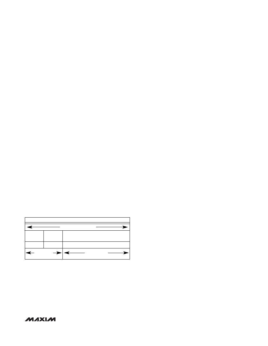
MSB ..................................................................................LSB
16 Bits of Serial Data
Control
Bits
Data Bits
MSB.............................................LSB
A1
A0
C1
C0
D11................................................D0
12 Data Bits
4 Address/
Control Bits
Address
Bits
Figure 7. Serial-Data Format (MSB Sent First)
相关PDF资料 |
PDF描述 |
|---|---|
| MAX536BCPE+ | IC DAC QUAD CALBRTD 12BIT 16-DIP |
| DS1091LUA-10A/V+ | IC ECONOSCILLATOR SS 8UMAX |
| PX0820/S | CONN PLUG 25POS W/O SOCKET BLACK |
| DS1091LUA-033+ | IC ECONOSCILLATOR SS 8-USOP |
| PX0410/04S/4550 | CONN SOCKET 4POS FEMALE RED |
相关代理商/技术参数 |
参数描述 |
|---|---|
| MAX536BCWE+ | 功能描述:数模转换器- DAC 12-Bit 4Ch Precision DAC RoHS:否 制造商:Texas Instruments 转换器数量:1 DAC 输出端数量:1 转换速率:2 MSPs 分辨率:16 bit 接口类型:QSPI, SPI, Serial (3-Wire, Microwire) 稳定时间:1 us 最大工作温度:+ 85 C 安装风格:SMD/SMT 封装 / 箱体:SOIC-14 封装:Tube |
| MAX536BCWE+T | 功能描述:数模转换器- DAC 12-Bit 4Ch Precision DAC RoHS:否 制造商:Texas Instruments 转换器数量:1 DAC 输出端数量:1 转换速率:2 MSPs 分辨率:16 bit 接口类型:QSPI, SPI, Serial (3-Wire, Microwire) 稳定时间:1 us 最大工作温度:+ 85 C 安装风格:SMD/SMT 封装 / 箱体:SOIC-14 封装:Tube |
| MAX536BCWE-T | 功能描述:数模转换器- DAC 12-Bit 4Ch Precision DAC RoHS:否 制造商:Texas Instruments 转换器数量:1 DAC 输出端数量:1 转换速率:2 MSPs 分辨率:16 bit 接口类型:QSPI, SPI, Serial (3-Wire, Microwire) 稳定时间:1 us 最大工作温度:+ 85 C 安装风格:SMD/SMT 封装 / 箱体:SOIC-14 封装:Tube |
| MAX536BEPE | 功能描述:数模转换器- DAC RoHS:否 制造商:Texas Instruments 转换器数量:1 DAC 输出端数量:1 转换速率:2 MSPs 分辨率:16 bit 接口类型:QSPI, SPI, Serial (3-Wire, Microwire) 稳定时间:1 us 最大工作温度:+ 85 C 安装风格:SMD/SMT 封装 / 箱体:SOIC-14 封装:Tube |
| MAX536BEPE+ | 功能描述:数模转换器- DAC 12-Bit 4Ch Precision DAC RoHS:否 制造商:Texas Instruments 转换器数量:1 DAC 输出端数量:1 转换速率:2 MSPs 分辨率:16 bit 接口类型:QSPI, SPI, Serial (3-Wire, Microwire) 稳定时间:1 us 最大工作温度:+ 85 C 安装风格:SMD/SMT 封装 / 箱体:SOIC-14 封装:Tube |
发布紧急采购,3分钟左右您将得到回复。