- 您现在的位置:买卖IC网 > PDF目录9188 > MAX5395MATA+T (Maxim Integrated Products)IC DGTL POT 256POS 50KOHM 8TDFN PDF资料下载
参数资料
| 型号: | MAX5395MATA+T |
| 厂商: | Maxim Integrated Products |
| 文件页数: | 2/17页 |
| 文件大小: | 0K |
| 描述: | IC DGTL POT 256POS 50KOHM 8TDFN |
| 标准包装: | 2,500 |
| 接片: | 256 |
| 电阻(欧姆): | 50k |
| 电路数: | 1 |
| 温度系数: | 标准值 50 ppm/°C |
| 存储器类型: | 易失 |
| 接口: | I²C |
| 电源电压: | 1.7 V ~ 5.5 V |
| 工作温度: | -40°C ~ 125°C |
| 安装类型: | * |
| 封装/外壳: | * |
| 供应商设备封装: | * |
| 包装: | * |
10
Maxim Integrated
MAX5395
Single, 256-Tap Volatile, I2C, Low-Voltage Linear
Taper Digital Potentiometer
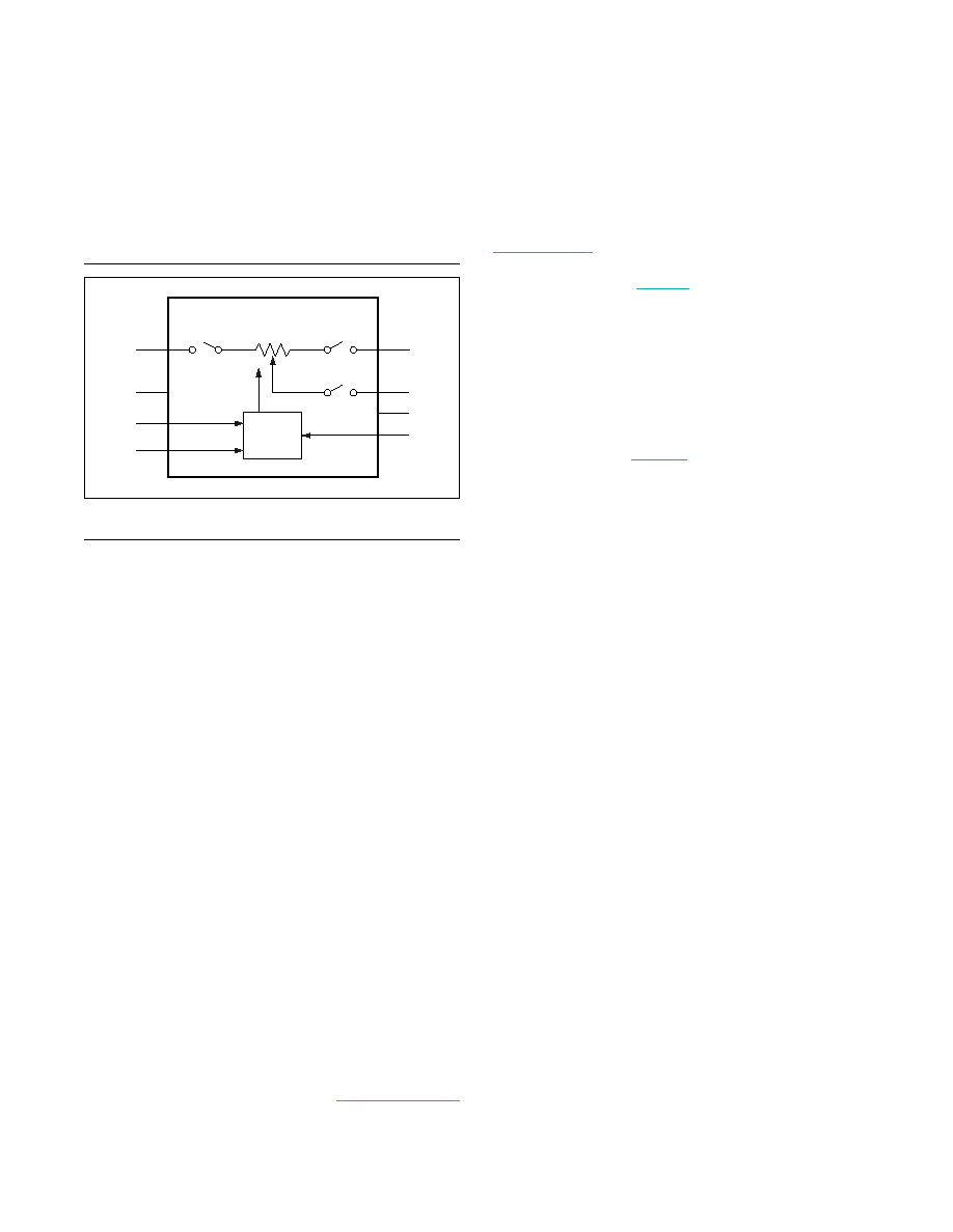
Functional Diagram
Detailed Description
The MAX5395 single, 256-tap volatile, low-voltage
linear taper digital potentiometer offers three end-to-
end resistance values of 10k
, 50k, and 100k.
Potentiometer terminals are independent of supply for
voltages up to +5.25V with single-supply operation from
1.7V to 5.5V (charge pump enabled). User-controlled
shutdown modes allow the H, W, or L terminals to
be opened with the wiper position set to zero-code,
midcode, full-code, or the value contained in the wiper
register. Ultra-low-quiescent supply current (< 1A) can
be achieved for supply voltages between 2.6V and 5.5V
by disabling the internal charge pump and not allowing
potentiometer terminals to exceed the supply voltage by
more than 0.3V. The MAX5395 provides a low 50ppm/°C
end-to-end temperature coefficient and features a I2C
serial interface.
The small package size, low supply operating voltage,
low supply current, and automotive temperature range
of the MAX5395 make the device uniquely suited for the
portable consumer market, battery-backup industrial
applications, and automotive market.
Charge Pump
The MAX5395 contains an internal charge pump that
guarantees the maximum wiper resistance, RWL, to be
less than 50
(25 typ) for supply voltages down to
1.7V and allows pins H, W, and L to be driven between
GND and 5.25V independent of VDD. Minimal charge-
pump feedthrough is present at the terminal outputs
and is illustrated by the Charge-Pump Feedthrough
at W vs. Frequency graph in the Typical Operating
Characteristics. The charge pump is on by default but
can be disabled with QP_OFF and enabled with the
QP_ON commands (Table 1). The MAX5395 minimum
supply voltage with charge pump disabled is limited
to 2.6V and terminal voltage cannot exceed -0.3V to
(VDD + 0.3V).
I2C Interface
The MAX5395 feature an I2C/SMBus-compatible, 2-wire
serial interface consisting of a serial data line (SDA) and
a serial clock line (SCL). SDA and SCL enable commu-
nication between the MAX5395 and the master at clock
rates up to 400kHz. Figure 1 shows the 2-wire interface
timing diagram. The master generates SCL and initiates
data transfer on the bus. The master device writes data
to the MAX5395 by transmitting the proper slave address
followed by the command byte and then the data word.
Each transmit sequence is framed by a START (S) or
Repeated START (Sr) condition and a STOP (P) condi-
tion. Each word transmitted to the MAX5395 is 8 bits long
and is followed by an acknowledge clock pulse. A master
reading data from the MAX5395 must transmit the proper
slave address followed by a series of nine SCL pulses for
each byte of data requested. The MAX5395 transmit data
on SDA in sync with the master-generated SCL pulses.
The master acknowledges receipt of each byte of data.
Each read sequence is framed by a START or Repeated
START condition, a not acknowledge, and a STOP condi-
tion. SDA operates as both an input and an open-drain
output. A pullup resistor, typically 4.7kI, is required on
SDA. SCL operates only as an input. A pullup resistor,
typically 4.7kI, is required on SCL if there are multiple
masters on the bus, or if the single master has an open-
drain SCL output.
Series resistors in line with SDA and SCL are optional.
Series resistors protect the digital inputs of the MAX5395
from high voltage spikes on the bus lines and mini-
mize crosstalk and undershoot of the bus signals. The
MAX5395 can accommodate bus voltages higher than
VDD up to a limit of +5.5V. Bus voltages lower than VDD
are not recommended and may result in significantly
increased interface currents and data corruption.
The MAX5395 with I2C interface contains a shift register
that decodes the command and address bytes, routing
the data to the register. Data written to a memory register
immediately updates the wiper position. The wiper pow-
ers up in mid position, D[7:0] = 0x80 with charge pump
enabled.
H
L
ADDRO
GND
SDA
W
VDD
SCL
MAX5395
I2C
INTERFACE
相关PDF资料 |
PDF描述 |
|---|---|
| MS3450L28-9PZ | CONN RCPT 12POS WALL MNT W/PINS |
| V24A48H300BF | CONVERTER MOD DC/DC 48V 300W |
| MAX5395LATA+T | IC DGTL POT 256POS 10KOHM 8TDFN |
| V24A48H300BL3 | CONVERTER MOD DC/DC 48V 300W |
| MS3450L28-9PY | CONN RCPT 12POS WALL MNT W/PINS |
相关代理商/技术参数 |
参数描述 |
|---|---|
| MAX5395NATA+T | 功能描述:数字电位计 IC Sgl 256-tap Volatile DigiPot w/SPI RoHS:否 制造商:Maxim Integrated 电阻:200 Ohms 温度系数:35 PPM / C 容差:25 % POT 数量:Dual 每 POT 分接头:256 弧刷存储器:Volatile 缓冲刷: 数字接口:Serial (3-Wire, SPI) 描述/功能:Dual Volatile Low Voltage Linear Taper Digital Potentiometer 工作电源电压:1.7 V to 5.5 V 电源电流:27 uA 最大工作温度:+ 125 C 安装风格:SMD/SMT 封装 / 箱体:TQFN-16 封装:Reel |
| MAX539ACPA | 功能描述:数模转换器- DAC RoHS:否 制造商:Texas Instruments 转换器数量:1 DAC 输出端数量:1 转换速率:2 MSPs 分辨率:16 bit 接口类型:QSPI, SPI, Serial (3-Wire, Microwire) 稳定时间:1 us 最大工作温度:+ 85 C 安装风格:SMD/SMT 封装 / 箱体:SOIC-14 封装:Tube |
| MAX539ACPA+ | 功能描述:数模转换器- DAC 12-Bit Precision DAC RoHS:否 制造商:Texas Instruments 转换器数量:1 DAC 输出端数量:1 转换速率:2 MSPs 分辨率:16 bit 接口类型:QSPI, SPI, Serial (3-Wire, Microwire) 稳定时间:1 us 最大工作温度:+ 85 C 安装风格:SMD/SMT 封装 / 箱体:SOIC-14 封装:Tube |
| MAX539ACSA | 功能描述:数模转换器- DAC RoHS:否 制造商:Texas Instruments 转换器数量:1 DAC 输出端数量:1 转换速率:2 MSPs 分辨率:16 bit 接口类型:QSPI, SPI, Serial (3-Wire, Microwire) 稳定时间:1 us 最大工作温度:+ 85 C 安装风格:SMD/SMT 封装 / 箱体:SOIC-14 封装:Tube |
| MAX539ACSA+ | 功能描述:数模转换器- DAC 12-Bit Precision DAC RoHS:否 制造商:Texas Instruments 转换器数量:1 DAC 输出端数量:1 转换速率:2 MSPs 分辨率:16 bit 接口类型:QSPI, SPI, Serial (3-Wire, Microwire) 稳定时间:1 us 最大工作温度:+ 85 C 安装风格:SMD/SMT 封装 / 箱体:SOIC-14 封装:Tube |
发布紧急采购,3分钟左右您将得到回复。