- 您现在的位置:买卖IC网 > PDF目录9188 > MAX5434MEZT+T (Maxim Integrated Products)IC POT DGTL 32TAP NV TSOT23-6 PDF资料下载
参数资料
| 型号: | MAX5434MEZT+T |
| 厂商: | Maxim Integrated Products |
| 文件页数: | 14/19页 |
| 文件大小: | 0K |
| 描述: | IC POT DGTL 32TAP NV TSOT23-6 |
| 产品培训模块: | Lead (SnPb) Finish for COTS Obsolescence Mitigation Program |
| 标准包装: | 2,500 |
| 接片: | 32 |
| 电阻(欧姆): | 50k |
| 电路数: | 1 |
| 温度系数: | 标准值 35 ppm/°C |
| 存储器类型: | 非易失 |
| 接口: | I²C(设备位址) |
| 电源电压: | 2.7 V ~ 5.25 V |
| 工作温度: | -40°C ~ 85°C |
| 安装类型: | 表面贴装 |
| 封装/外壳: | SOT-23-6 细型,TSOT-23-6 |
| 供应商设备封装: | TSOT-23-6 |
| 包装: | 带卷 (TR) |
MAX5432–MAX5435
32-Tap, Nonvolatile, I2C, Linear, Digital
Potentiometers
4
_______________________________________________________________________________________
TIMING CHARACTERISTICS (continued)
(VDD = +2.7V to +5.25V, VH = VDD, VL = GND, TA = -40°C to +85°C, unless otherwise noted. Typical values are at VDD = +5V, TA =
+25°C.) (Figures 1 and 2) (Note 1)
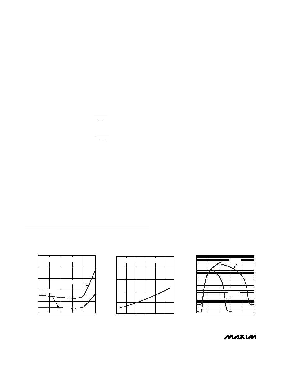
Typical Operating Characteristics
(VDD = +5V, TA = +25°C, unless otherwise noted.)
0
0.3
0.9
0.6
1.2
1.5
-40
10
-15
35
60
85
STANDBY SUPPLY CURRENT
vs. TEMPERATURE
MAX5432–35
toc01
TEMPERATURE (
°C)
SUPPLY
CURRENT
(
A)
DIGITAL INPUTS = GND OR VDD
VDD = 5V
VDD = 3V
0
0.2
0.6
0.4
0.8
1.0
2.5
3.5
3.0
4.0
4.5
5.0
5.5
SUPPLY CURRENT
vs. SUPPLY VOLTAGE
MAX5432–35
toc02
SUPPLY VOLTAGE (V)
SUPPLY
CURRENT
(
A)
DIGITAL INPUTS = GND OR VDD
02
13
5
SUPPLY CURRENT
vs. DIGITAL INPUT VOLTAGE
MAX5432–35
toc03
DIGITAL INPUT VOLTAGE (V)
SUPPLY
CURRENT
(
A)
1000
0.1
1
10
100
VDD = 5V
VDD = 3V
4
VV
V
WH
H
-
31
.
VV
V
WL
H
-
31
.
Note 2: The DNL and INL are measured with the potentiometer configured as a variable resistor. For the 3-terminal potentiometers
(MAX5432/MAX5433), H is unconnected and L = GND. At VDD = 5V, W is driven with a source current of 80A for the 50k
configuration, and 40A for the 100k
configuration. At VDD = 3V, W is driven with a source current of 40A for the 50k
configuration, and 20A for the 100k
configuration.
Note 3: The DNL and INL are measured with the potentiometer configured as a voltage-divider with H = VDD and L = GND
(MAX5432/MAX5433 only). The wiper terminal is unloaded and measured with an ideal voltmeter.
Note 4: Full-scale error is defined as
Note 5: Zero-scale error is defined as
Note 6: The wiper resistance is the worst value measured by injecting the currents given in Note 2 into W with L = GND.
RW = (VW - VH) / IW.
Note 7: The device draws current in excess of the specified supply current when the digital inputs are driven with voltages between
(VDD - 0.5V) and (GND + 0.5V). See the Supply Current vs. Digital Input Voltage graph in the Typical Operating Characteristics.
Note 8: Wiper is at midscale with a 10pF capacitive load. Potentiometer set to midscale, L = GND, an AC source is applied to H,
and the output is measured as 3dB lower than the DC W/H value in dB.
Note 9: This is measured from the STOP pulse to the time it takes the output to reach 50% of the output step size (divider mode). It
is measured with a maximum external capacitive load of 10pF.
Note 10: The programming current exists only during NV writes (12ms typ).
Note 11: Digital timing is guaranteed by design and characterization, and is not production tested.
Note 12: An appropriate bus pullup resistance must be selected depending on board capacitance. Refer to the I
2C-bus specifica-
tion document linked to this web address: www.semiconductors.philips.com/acrobat/literature/9398/39340011.pdf
Note 13: The idle time begins from the initiation of the stop pulse.
相关PDF资料 |
PDF描述 |
|---|---|
| MAX5433META+T | IC POT DGTL 32-TAP NV I2C 8-TDFN |
| MAX5432META+T | IC POT DGTL 32-TAP NV I2C 8-TDFN |
| MAX5160LEUA+T | IC POT DGTL LO PWR 32 TAP 8-UMAX |
| MAX5160MEUA+T | IC POT DGTL LO PWR 32 TAP 8-UMAX |
| VI-24X-MW | CONVERTER MOD DC/DC 5.2V 100W |
相关代理商/技术参数 |
参数描述 |
|---|---|
| MAX5434NEKT-T | 制造商:Maxim Integrated Products 功能描述:32-TAP, NONVOLATILE, I2C, LINEAR, DIGITAL POT - Tape and Reel |
| MAX5434NEZ | 制造商:Rochester Electronics LLC 功能描述: 制造商:Maxim Integrated Products 功能描述: |
| MAX5434NEZT | 制造商:Maxim Integrated Products 功能描述:32-TAP NONVOLATILE I2C LINEAR D - Cut Tape Product |
| MAX5434NEZT+ | 制造商:Maxim Integrated Products 功能描述:DGTL POTENTIOMETER 32POS 50KOHM SGL 6PIN TSOT-23 - Rail/Tube |
| MAX5434NEZT+T | 功能描述:数字电位计 IC 32-Tap Nonvolatile I2C Linear RoHS:否 制造商:Maxim Integrated 电阻:200 Ohms 温度系数:35 PPM / C 容差:25 % POT 数量:Dual 每 POT 分接头:256 弧刷存储器:Volatile 缓冲刷: 数字接口:Serial (3-Wire, SPI) 描述/功能:Dual Volatile Low Voltage Linear Taper Digital Potentiometer 工作电源电压:1.7 V to 5.5 V 电源电流:27 uA 最大工作温度:+ 125 C 安装风格:SMD/SMT 封装 / 箱体:TQFN-16 封装:Reel |
发布紧急采购,3分钟左右您将得到回复。