- 您现在的位置:买卖IC网 > PDF目录8538 > MAX5520ETC+T (Maxim Integrated Products)IC DAC 10BIT SGL ULP 12-TQFN PDF资料下载
参数资料
| 型号: | MAX5520ETC+T |
| 厂商: | Maxim Integrated Products |
| 文件页数: | 7/20页 |
| 文件大小: | 0K |
| 描述: | IC DAC 10BIT SGL ULP 12-TQFN |
| 产品培训模块: | Lead (SnPb) Finish for COTS Obsolescence Mitigation Program |
| 标准包装: | 2,500 |
| 设置时间: | 660µs |
| 位数: | 10 |
| 数据接口: | MICROWIRE?,QSPI?,串行,SPI? |
| 转换器数目: | 1 |
| 电压电源: | 单电源 |
| 工作温度: | -40°C ~ 85°C |
| 安装类型: | 表面贴装 |
| 封装/外壳: | 12-WQFN 裸露焊盘 |
| 供应商设备封装: | 12-TQFN-EP(4x4) |
| 包装: | 带卷 (TR) |
| 输出数目和类型: | 1 电压,单极;1 电压,双极 |
| 采样率(每秒): | * |
MAX5520/MAX5521
+1.8V to +5.5V, Ultra-Low-Power, 10-Bit,
Voltage-Output DACs
______________________________________________________________________________________
15
Power Modes
The MAX5520/MAX5521 feature two power modes to
conserve power during idle periods. In normal opera-
tion, the device is fully operational. In shutdown mode,
the device is completely powered down, including the
internal voltage reference in the MAX5521. The
MAX5521 also offers a standby mode where all circuitry
is powered down except the internal voltage reference.
Standby mode keeps the reference powered up while
the remaining circuitry is shut down, allowing it to be
used as a system reference. Standby mode also helps
reduce the wake-up delay by not requiring the refer-
ence to power up when returning to normal operation.
Shutdown Mode
The MAX5520/MAX5521 feature a software-program-
mable shutdown mode that reduces the typical supply
current and the reference input current to 0.18A
(max). Writing an input control word with control bits
C[3:0] = 1110 places the device in shutdown mode
(Table 2). In shutdown, the MAX5520 reference input
and DAC output buffers go high impedance. Placing
the MAX5521 into shutdown turns off the internal refer-
ence, and the DAC output buffers go high impedance.
The serial interface remains active for all devices.
Table 2 shows several commands that bring the
MAX5520/MAX5521 back to normal operation. The
power-up time from shutdown is required before the
DAC outputs are valid.
Note: For the MAX5521, standby mode cannot be
entered directly from shutdown mode. The device must
be brought into normal operation before entering stand-
by mode.
Standby Mode (MAX5521 Only)
The MAX5521 features a software-programmable
standby mode that reduces the typical supply current
to 6A. Standby mode powers down all circuitry except
the internal voltage reference. Place the device in
standby mode by writing an input control word with
control bits C[3:0] = 1100 (Table 2). The internal refer-
ence and serial interface remain active while the DAC
output buffers go high impedance. If the MAX5521 is
coming out of standby, the power-up time from standby
is required before the DAC outputs are valid.
For the MAX5521, standby mode cannot be entered
directly from shutdown mode. The device must be
brought into normal operation before entering standby
mode. To enter standby from shutdown, issue the com-
mand to return to normal operation, followed immedi-
ately by the command to go into standby.
Table 2 shows several commands that bring the
MAX5521 back to normal operation. When transition-
ing from standby mode to normal operation, only the
DAC power-up time is required before the DAC outputs
are valid.
Reference Input
The MAX5520 accepts a reference with a voltage range
extending from 0 to VDD. The output voltage (VOUT) is
represented by a digitally programmable voltage
source as:
VOUT = (VREF x N / 1024) x gain
where N is the numeric value of the DAC’s binary input
code (0 to 1023), VREF is the reference voltage and
gain is the externally set voltage gain for the MAX5520/
MAX5521.
In shutdown mode, the reference input enters a high-
impedance state with an input impedance of 2.5G (typ).
Reference Output
The MAX5521 internal voltage reference is software
configurable to one of four voltages. Upon power-up,
the default reference voltage is 1.214V. Configure the
reference voltage using the D8 and D9 data bits (Table
3) when the control bits are as follows: C[3:0] = 1100,
1101, or 1110 (Table 2). VDD must be kept at a mini-
mum of 200mV above VREF for proper operation.
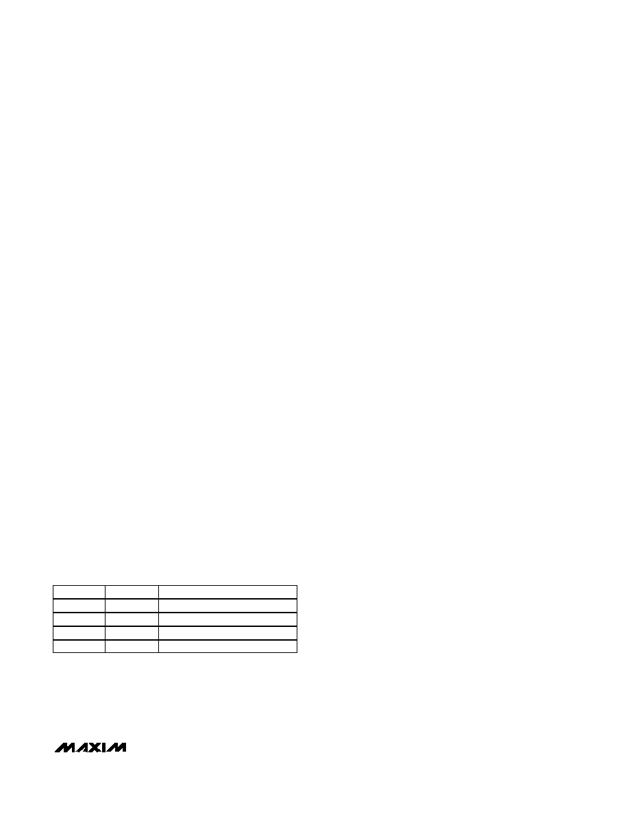
D9
D8
REFERENCE VOLTAGE (V)
00
1.214
01
1.940
10
2.425
11
3.885
Table 3. Reference Output Voltage
Programming
相关PDF资料 |
PDF描述 |
|---|---|
| MAX5514ETC+ | IC DAC 8BIT DUAL VOUT 12TQFN |
| 3-1877845-8 | PLUG 5POS 0 DEG BLK/YEL 4.0-5.2 |
| 3-1877845-2 | PLUG 5POS 0 DEG GRY/WH 4.0-5.2 |
| VE-JWW-MW-S | CONVERTER MOD DC/DC 5.5V 100W |
| MAX5514ETC+T | IC DAC 8BIT DUAL VOUT 12TQFN |
相关代理商/技术参数 |
参数描述 |
|---|---|
| MAX5521ETC | 功能描述:数模转换器- DAC RoHS:否 制造商:Texas Instruments 转换器数量:1 DAC 输出端数量:1 转换速率:2 MSPs 分辨率:16 bit 接口类型:QSPI, SPI, Serial (3-Wire, Microwire) 稳定时间:1 us 最大工作温度:+ 85 C 安装风格:SMD/SMT 封装 / 箱体:SOIC-14 封装:Tube |
| MAX5521ETC+ | 功能描述:数模转换器- DAC 10-Bit Precision DAC RoHS:否 制造商:Texas Instruments 转换器数量:1 DAC 输出端数量:1 转换速率:2 MSPs 分辨率:16 bit 接口类型:QSPI, SPI, Serial (3-Wire, Microwire) 稳定时间:1 us 最大工作温度:+ 85 C 安装风格:SMD/SMT 封装 / 箱体:SOIC-14 封装:Tube |
| MAX5521ETC+T | 功能描述:数模转换器- DAC 10-Bit Precision DAC RoHS:否 制造商:Texas Instruments 转换器数量:1 DAC 输出端数量:1 转换速率:2 MSPs 分辨率:16 bit 接口类型:QSPI, SPI, Serial (3-Wire, Microwire) 稳定时间:1 us 最大工作温度:+ 85 C 安装风格:SMD/SMT 封装 / 箱体:SOIC-14 封装:Tube |
| MAX5521ETC-T | 功能描述:数模转换器- DAC RoHS:否 制造商:Texas Instruments 转换器数量:1 DAC 输出端数量:1 转换速率:2 MSPs 分辨率:16 bit 接口类型:QSPI, SPI, Serial (3-Wire, Microwire) 稳定时间:1 us 最大工作温度:+ 85 C 安装风格:SMD/SMT 封装 / 箱体:SOIC-14 封装:Tube |
| MAX5522EUA | 功能描述:数模转换器- DAC RoHS:否 制造商:Texas Instruments 转换器数量:1 DAC 输出端数量:1 转换速率:2 MSPs 分辨率:16 bit 接口类型:QSPI, SPI, Serial (3-Wire, Microwire) 稳定时间:1 us 最大工作温度:+ 85 C 安装风格:SMD/SMT 封装 / 箱体:SOIC-14 封装:Tube |
发布紧急采购,3分钟左右您将得到回复。