- 您现在的位置:买卖IC网 > PDF目录17047 > MAX5535EVKIT+ (Maxim Integrated Products)KIT EVALUATION FOR MAX5535 PDF资料下载
参数资料
| 型号: | MAX5535EVKIT+ |
| 厂商: | Maxim Integrated Products |
| 文件页数: | 11/24页 |
| 文件大小: | 0K |
| 描述: | KIT EVALUATION FOR MAX5535 |
| 产品培训模块: | Lead (SnPb) Finish for COTS Obsolescence Mitigation Program |
| 标准包装: | 1 |
| DAC 的数量: | 2 |
| 位数: | 12 |
| 数据接口: | 串行 |
| 设置时间: | 660µs |
| DAC 型: | 电压 |
| 工作温度: | -40°C ~ 85°C |
| 已供物品: | 板,CD |
| 已用 IC / 零件: | MAX5535 |
MAX5532–MAX5535
Dual, Ultra-Low-Power,
12-Bit, Voltage-Output DACs
______________________________________________________________________________________
19
Voltage Biasing a
Current-Output Transducer
See the circuit in Figure 5 for an illustration of how to
configure the MAX5534/MAX5535 to bias a current-out-
put transducer. In Figure 5, the output voltage of the
MAX5534/MAX5535 is a function of the voltage drop
across the transducer added to the voltage drop
across the feedback resistor R.
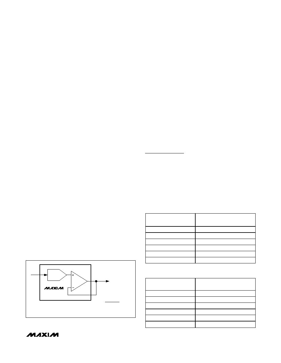
Unipolar Output
Figure 6 shows the MAX5534 in a unipolar output con-
figuration with unity gain. Table 4 lists the unipolar out-
put codes.
Bipolar Output
The MAX5534 output can be configured for bipolar
operation as shown in Figure 7. The output voltage is
given by the following equation:
VOUT_ = VREFIN x [(NA - 2048) / 2048]
where NA represents the decimal value of the DAC’s
binary input code. Table 5 shows the digital codes (off-
set binary) and the corresponding output voltage for
the circuit in Figure 7.
Configurable Output Gain
The MAX5534/MAX5535 have force-sense outputs,
which provide a connection directly to the inverting termi-
nal of the output op-amp, yielding the most flexibility. The
advantage of the force-sense output is that specific gains
can be set externally for a given application. The gain
error for the MAX5534/MAX5535 is specified in a unity-
gain configuration (op-amp output and inverting termi-
nals connected), and additional gain error results from
external resistor tolerances. Another advantage of the
force-sense DAC is that it allows many useful circuits to
be created with only a few simple external components.
An example of a custom fixed gain using the MAX5534/
MAX5535 force-sense output is shown in Figure 8. In
this example, R1 and R2 set the gain for VOUTA.
VOUTA = [(VREFIN x NA) / 4096] x [1 + (R2 / R1)]
where NA represents the numeric value of the DAC
input code.
Self-Biased Two-Electrode
Potentiostat Application
See the circuit in Figure 10 for an illustration of how to
use the MAX5535 to bias a two-electrode potentiostat
on the input of an ADC.
Power Supply and
Bypassing Considerations
Bypass the power supply with a 0.1F capacitor to GND.
Minimize lengths to reduce lead inductance. If noise
becomes an issue, use shielding and/or ferrite beads to
increase isolation. For the thin QFN package, connect the
exposed pad to ground.
Layout Considerations
Digital and AC transient signals coupling to GND can
create noise at the output. Use proper grounding tech-
niques, such as a multilayer board with a low-inductance
ground plane. Wire-wrapped boards and sockets are not
recommended. For optimum system performance, use
printed circuit (PC) boards. Good PC board ground lay-
out minimizes crosstalk between DAC outputs, reference
inputs, and digital inputs. Reduce crosstalk by keeping
analog lines away from digital lines.
Table 4. Unipolar Code Table (Gain = +1)
DAC CONTENTS
MSB
LSB
ANALOG OUTPUT
1111
+VREF (4095/4096)
1000
0000
0001
+VREF (2049/4096)
1000
0000
+VREF (2048/4096) = +VREF / 2
0111
1111
+VREF (2047/4096)
0000
0001
+VREF (1/4096)
0000
0V
Table 5. Bipolar Code Table (Gain = +1)
DAC CONTENTS
MSB
LSB
ANALOG OUTPUT
1111
+VREF (2047/2048)
1000
0000
0001
+VREF (1/2048)
1000
0000
0V
0111
1111
-VREF (1/2048)
0000
0001
-VREF (2047/2048)
0000
-VREF (2048/2048) = -VREF
NA IS THE DAC INPUT CODE
(0 TO 4095 DECIMAL).
REFIN
MAX5534
OUT_
FB_
VOUT =
VREFIN
× NA
4096
DAC
Figure 6. Unipolar Output Circuit
相关PDF资料 |
PDF描述 |
|---|---|
| MAX5890EVKIT# | KIT EVALUATION FOR MAX5890 |
| MLG1005SR27J | INDUCTOR MULTILAYER 270NH 0402 |
| EEC36DREF | CONN EDGECARD 72POS .100 EYELET |
| ECC19DRTH-S13 | CONN EDGECARD 38POS .100 EXTEND |
| HKQ0603S2N8C-T | INDUCTOR HI FREQ 2.8NH 0201 |
相关代理商/技术参数 |
参数描述 |
|---|---|
| MAX5535EVKIT+ | 功能描述:数据转换 IC 开发工具 MAX5535 Eval Kit RoHS:否 制造商:Texas Instruments 产品:Demonstration Kits 类型:ADC 工具用于评估:ADS130E08 接口类型:SPI 工作电源电压:- 6 V to + 6 V |
| MAX5541CSA | 功能描述:数模转换器- DAC RoHS:否 制造商:Texas Instruments 转换器数量:1 DAC 输出端数量:1 转换速率:2 MSPs 分辨率:16 bit 接口类型:QSPI, SPI, Serial (3-Wire, Microwire) 稳定时间:1 us 最大工作温度:+ 85 C 安装风格:SMD/SMT 封装 / 箱体:SOIC-14 封装:Tube |
| MAX5541CSA+ | 功能描述:数模转换器- DAC 16-Bit Precision DAC RoHS:否 制造商:Texas Instruments 转换器数量:1 DAC 输出端数量:1 转换速率:2 MSPs 分辨率:16 bit 接口类型:QSPI, SPI, Serial (3-Wire, Microwire) 稳定时间:1 us 最大工作温度:+ 85 C 安装风格:SMD/SMT 封装 / 箱体:SOIC-14 封装:Tube |
| MAX5541CSA+T | 功能描述:数模转换器- DAC 16-Bit Precision DAC RoHS:否 制造商:Texas Instruments 转换器数量:1 DAC 输出端数量:1 转换速率:2 MSPs 分辨率:16 bit 接口类型:QSPI, SPI, Serial (3-Wire, Microwire) 稳定时间:1 us 最大工作温度:+ 85 C 安装风格:SMD/SMT 封装 / 箱体:SOIC-14 封装:Tube |
| MAX5541CSA-T | 功能描述:数模转换器- DAC RoHS:否 制造商:Texas Instruments 转换器数量:1 DAC 输出端数量:1 转换速率:2 MSPs 分辨率:16 bit 接口类型:QSPI, SPI, Serial (3-Wire, Microwire) 稳定时间:1 us 最大工作温度:+ 85 C 安装风格:SMD/SMT 封装 / 箱体:SOIC-14 封装:Tube |
发布紧急采购,3分钟左右您将得到回复。