- 您现在的位置:买卖IC网 > PDF目录9795 > MAX562CWI+T (Maxim Integrated Products)IC INTERFACE SER NOTEBOOK 28SOIC PDF资料下载
参数资料
| 型号: | MAX562CWI+T |
| 厂商: | Maxim Integrated Products |
| 文件页数: | 6/8页 |
| 文件大小: | 0K |
| 描述: | IC INTERFACE SER NOTEBOOK 28SOIC |
| 产品培训模块: | Lead (SnPb) Finish for COTS Obsolescence Mitigation Program |
| 标准包装: | 1,000 |
| 类型: | 收发器 |
| 驱动器/接收器数: | 3/5 |
| 规程: | RS232 |
| 电源电压: | 2.7 V ~ 5.25 V |
| 安装类型: | 表面贴装 |
| 封装/外壳: | 28-SOIC(0.295",7.50mm 宽) |
| 供应商设备封装: | 28-SOIC W |
| 包装: | 带卷 (TR) |
MAX562
Complete 230kbps, 2.7V to 5.25V
Serial Interface for Notebook Computers
6
_______________________________________________________________________________________
_______________Detailed Description
The MAX562 has three sections: the charge-pump voltage
converter, the drivers (transmitters), and the receivers.
Charge-Pump Voltage Converter
The charge-pump voltage converter is used to produce a
positive and a negative supply to drive the transmitters. The
positive voltage (V+) is generated by a regulated charge
pump working as either a doubler or a tripler (depending on
the VCC level) and using capacitors C1A, C1B and C3 (see
Typical Operating Circuit). The negative voltage (V-) derives
from V+ using a simple charge-pump inverter that employs
capacitors C2 and C4.
These charge-pump converters are regulated to give output
voltages of +5.8V and -5.2V. Having regulated supplies
generated on-chip makes the MAX562's performance insen-
sitive to variations in VCC from 2.7V to 5.25V, transmitter load-
ing changes, and operating temperature changes.
When
SHDN is low, the charge pumps are disabled, V+ is
internally connected to VCC, and V- is internally connected to
GND.
EIA/TIA-562 Drivers
The driver output voltage is guaranteed to meet the ±3.7V
EIA/TIA-562 specification over the full range of operating
temperatures and voltages, when each transmitter is
loaded with up to 3k
and operated up to 230kbps (see
Typical Operating Characteristics). The typical driver out-
put voltage swing exceeds ±4V with a 3k
load on all
transmitter outputs. The open-circuit output voltage swing
is typically from (V+ - 0.7V) to (V- + 0.7V). Output swing is
not significantly dependent on VCC since the charge
pumps are regulated.
Input thresholds are CMOS and TTL compatible. Connect
unused inputs to VCC or to GND.
When
SHDN is low, the driver outputs are off and their leak-
age currents are less than 10A, even if the transmitter
outputs are back-driven between -7V and +15V. Taking
SHDN low does not disable the receivers.
When
SHDN and EN are both low, the entire chip is
disabled and all outputs are high impedance. Power
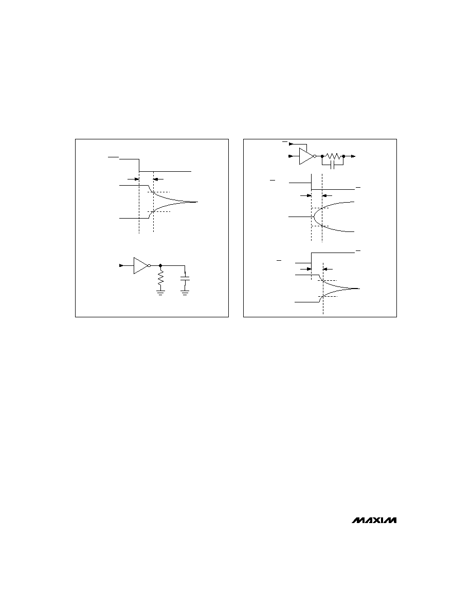
consumption is lowest in this condition. Exiting shutdown
takes about 100s, but depends on VCC. Figure 5 shows
SHDN
VOH
VOL
+3V
0V
OUTPUT DISABLE TIME (tDT)
+3V
-3V
0V
A. TIMING DIAGRAM
1 OR 0
TX
3k
50pF
B. TEST CIRCUIT
TRANSMITTER
OUTPUTS
Figure 3. Transmitter-Output Disable Timing
EN
VOH -1V,
VOL +1.6V
R_IN
R_OUT
1k
150pF
A. TEST CIRCUIT
B. ENABLE TIMING
EN INPUT
RECEIVER
OUTPUTS
+3V
0V
OUTPUT ENABLE TIME (tER)
VOH
VOL
EN
RECEIVER
OUTPUTS
EN
+3V
0V
OUTPUT DISABLE TIME (tDR)
VOH -0.5V
VOL +0.5V
EN INPUT
VOH
VOL
C. DISABLE TIMING
R_
Figure 4. Receiver-Output Enable and Disable Timing
相关PDF资料 |
PDF描述 |
|---|---|
| VI-23H-IU-F4 | CONVERTER MOD DC/DC 52V 200W |
| MAX206CWG+T | IC TXRX RS-232 W/CAP 24-SOIC |
| MS27473T22F35PA | CONN PLUG 100POS STRAIGHT W/PINS |
| MS27466E21B16P | CONN RCPT 16POS WALL MT W/PINS |
| MS27467T13F98SC | CONN PLUG 10POS STRAIGHT W/SCKT |
相关代理商/技术参数 |
参数描述 |
|---|---|
| MAX562EAI | 功能描述:RS-232接口集成电路 RoHS:否 制造商:Exar 数据速率:52 Mbps 工作电源电压:5 V 电源电流:300 mA 工作温度范围:- 40 C to + 85 C 安装风格:SMD/SMT 封装 / 箱体:LQFP-100 封装: |
| MAX562EAI+ | 功能描述:RS-232接口集成电路 230kbps 2.7-5.25V Serial Interface RoHS:否 制造商:Exar 数据速率:52 Mbps 工作电源电压:5 V 电源电流:300 mA 工作温度范围:- 40 C to + 85 C 安装风格:SMD/SMT 封装 / 箱体:LQFP-100 封装: |
| MAX562EAI+T | 功能描述:RS-232接口集成电路 230kbps 2.7-5.25V Serial Interface RoHS:否 制造商:Exar 数据速率:52 Mbps 工作电源电压:5 V 电源电流:300 mA 工作温度范围:- 40 C to + 85 C 安装风格:SMD/SMT 封装 / 箱体:LQFP-100 封装: |
| MAX562EAI-T | 功能描述:RS-232接口集成电路 RoHS:否 制造商:Exar 数据速率:52 Mbps 工作电源电压:5 V 电源电流:300 mA 工作温度范围:- 40 C to + 85 C 安装风格:SMD/SMT 封装 / 箱体:LQFP-100 封装: |
| MAX562EWI | 功能描述:RS-232接口集成电路 RoHS:否 制造商:Exar 数据速率:52 Mbps 工作电源电压:5 V 电源电流:300 mA 工作温度范围:- 40 C to + 85 C 安装风格:SMD/SMT 封装 / 箱体:LQFP-100 封装: |
发布紧急采购,3分钟左右您将得到回复。