- 您现在的位置:买卖IC网 > PDF目录2011 > MAX5839BCMH (Maxim Integrated Products)IC DAC OCTAL V-OUT 13BIT 44-MQFP PDF资料下载
参数资料
| 型号: | MAX5839BCMH |
| 厂商: | Maxim Integrated Products |
| 文件页数: | 2/16页 |
| 文件大小: | 0K |
| 描述: | IC DAC OCTAL V-OUT 13BIT 44-MQFP |
| 产品培训模块: | Lead (SnPb) Finish for COTS Obsolescence Mitigation Program |
| 标准包装: | 96 |
| 设置时间: | 22µs |
| 位数: | 13 |
| 数据接口: | 并联 |
| 转换器数目: | 8 |
| 电压电源: | 单电源 |
| 工作温度: | 0°C ~ 70°C |
| 安装类型: | 表面贴装 |
| 封装/外壳: | 44-QFP |
| 供应商设备封装: | 44-MQFP(10x10) |
| 包装: | 托盘 |
| 输出数目和类型: | 8 电压,单极;8 电压,双极 |
| 采样率(每秒): | * |
MAX5839
Octal, 13-Bit Voltage-Output DAC
with Parallel Interface
10
______________________________________________________________________________________
Digital Inputs and Interface Logic
All digital inputs are compatible with both TTL and
CMOS logic. The MAX5839 interfaces with micro-
processors using a data bus at least 13 bits wide. The
interface is double buffered, allowing simultaneous
updating of all DACs. There are two latches for each
DAC (see Functional Diagram): an input latch that
receives data from the data bus, and a DAC latch that
receives data from the input latch. Address lines A0,
A1, and A2 select which DAC’s input latch receives
data from the data bus, as shown in Table 1. Both the
input latches and the DAC latches are transparent
when CS, WR, and LD are all low. Any change of
D0–D12 during this condition appears at the output
instantly. Transfer data from the input latches to the
DAC latches by asserting the asynchronous LD signal.
Each DAC’s analog output reflects the data held in its
DAC latch. All control inputs are level triggered. Table 2
is an interface truth table.
Input Write Cycle
Data can be latched or transferred directly to the DAC.
CS and WR control the input latch, and LD transfers
information from the input latch to the DAC latch. The
input latch is transparent when CS and WR are low,
and the DAC latch is transparent when LD is low. The
address lines (A0, A1, A2) must be valid for the dura-
tion that CS and WR are low (Figure 1), to prevent data
from being inadvertently written to the wrong DAC.
Data is latched within the input latch when either CS or
WR is high.
Loading the DACs
Taking LD high latches data into the DAC latches. If LD
is brought low when WR and CS are low, the DAC
addressed by A0, A1, and A2 is directly controlled by
the data on D0–D12. This allows the maximum digital
update rate; however, it is sensitive to any glitches or
skew in the input data stream.
Asynchronous Clear
The MAX5839 has an asynchronous clear pin (CLR)
that, when asserted, sets all DAC outputs to the voltage
present on their respective DUTGND pins. Deassert
CLR to return the DAC output to its previous voltage.
Note that CLR does not clear any of the internal digital
registers.
Applications Information
Multiplying Operation
The MAX5839 can be used for multiplying applications.
Its reference accepts both DC and AC signals. Since
the reference inputs are unipolar, multiplying operation
is limited to two quadrants. See the graphs in the
Typical Operating Characteristics for dynamic perfor-
mance of the DACs and output buffers.
Digital Code and
Analog Output Voltage
The MAX5839 uses offset binary coding. A 13-bit two’s
complement code is converted to a 13-bit offset binary
code by adding 212 = 4096.
Output Voltage Range
For typical operation, connect DUTGND to signal
ground, VREF+ to +4.5V, and VREF- to -2.0V. Table 3
shows the relationship between digital code and output
voltage.
The DAC digital code controls each leg of the 13-bit
R-2R ladder. A code of 0x0 connects all legs of the lad-
der to REF-, corresponding to a DAC output voltage
(VDAC) equal to REF-. A code of 0x1FFF connects all
legs of the ladder to REF+, corresponding to a VDAC
approximately equal to REF+.
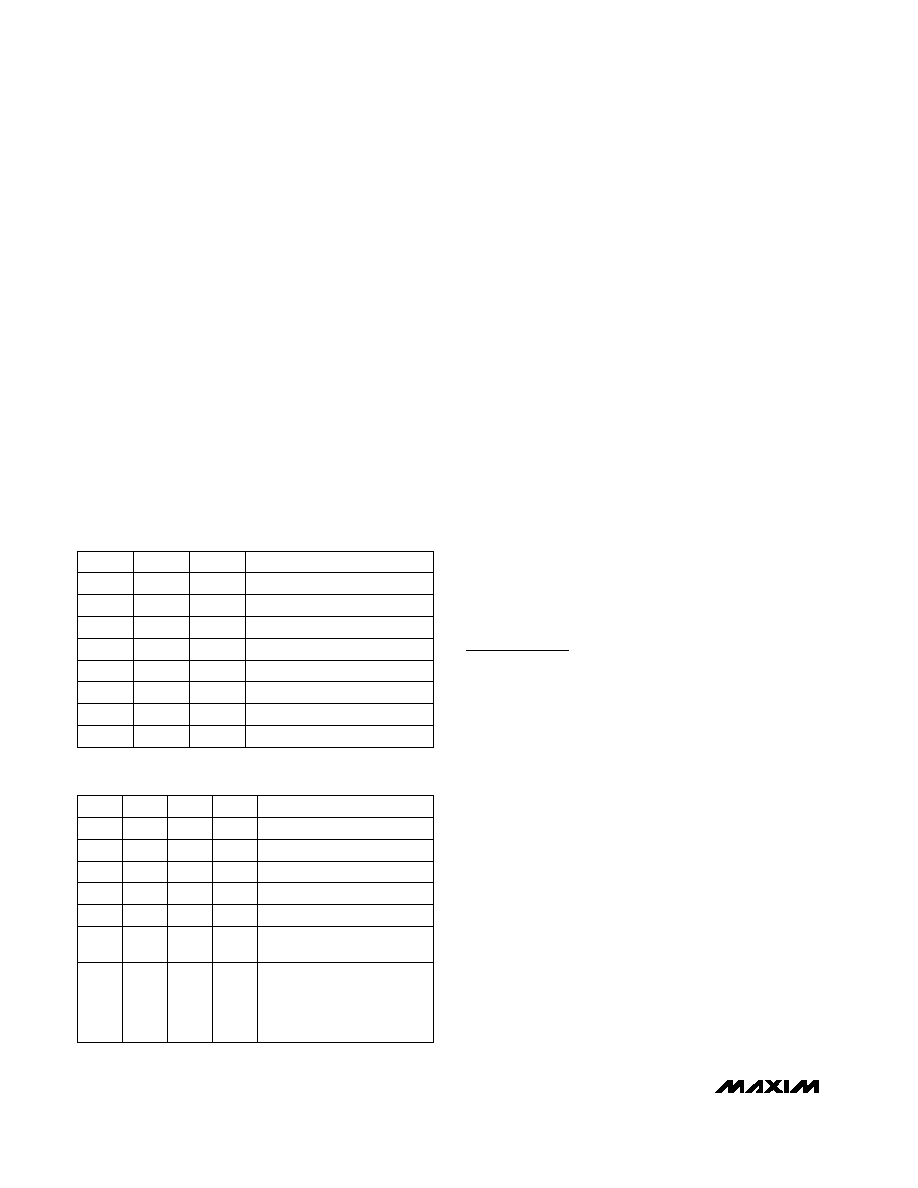
A2
FUNCTION
DAC A input latch
0
DAC C input latch
0
DAC B input latch
0
DAC D input latch
0
DAC H input latch
1
DAC E input latch
1
DAC G input latch
1
DAC F input latch
1
A1
1
0
1
0
1
0
A0
1
0
1
0
1
CLR
DAC register transparent
FUNCTION
X
Input register transparent
X
Input register latched
X
Input register latched
X
DAC register latched
X
Outputs of DACs set to volt-
age defined by the DAC
register, the references,
and the corresponding
DUTGND_ _
1
Outputs of DACs at
DUTGND_ _
0
LD
0
X
1
X
WR
X
0
1
X
Table 1. MAX5839 DAC Addressing
Table 2. Interface Truth Table
CS
X
0
X
1
X
X = Don’t care
相关PDF资料 |
PDF描述 |
|---|---|
| MAX5841MEUB+T | IC DAC 10BIT QUAD 2WIRE 10-UMAX |
| MAX5851ETL+T | IC DAC 8BIT DUAL 80MSPS 40-TQFN |
| MAX5852ETL+T | IC DAC 8BIT DUAL 165MSPS 40-TQFN |
| MAX5856AECM+D | IC DAC 8BIT DUAL 300MSPS 48-TQFP |
| MAX5858AECM+D | IC DAC 10BIT DUAL 300MSPS 48TQFP |
相关代理商/技术参数 |
参数描述 |
|---|---|
| MAX5839BEMH | 制造商:Maxim Integrated Products 功能描述:OCTAL, 13-BIT VOLTAGE-OUTPUT DAC WITH PARALLEL INTERFACE - Rail/Tube |
| MAX5841LEUB | 功能描述:数模转换器- DAC RoHS:否 制造商:Texas Instruments 转换器数量:1 DAC 输出端数量:1 转换速率:2 MSPs 分辨率:16 bit 接口类型:QSPI, SPI, Serial (3-Wire, Microwire) 稳定时间:1 us 最大工作温度:+ 85 C 安装风格:SMD/SMT 封装 / 箱体:SOIC-14 封装:Tube |
| MAX5841LEUB+ | 功能描述:数模转换器- DAC 10-Bit 4Ch Precision DAC RoHS:否 制造商:Texas Instruments 转换器数量:1 DAC 输出端数量:1 转换速率:2 MSPs 分辨率:16 bit 接口类型:QSPI, SPI, Serial (3-Wire, Microwire) 稳定时间:1 us 最大工作温度:+ 85 C 安装风格:SMD/SMT 封装 / 箱体:SOIC-14 封装:Tube |
| MAX5841LEUB+T | 功能描述:数模转换器- DAC 10-Bit 4Ch Precision DAC RoHS:否 制造商:Texas Instruments 转换器数量:1 DAC 输出端数量:1 转换速率:2 MSPs 分辨率:16 bit 接口类型:QSPI, SPI, Serial (3-Wire, Microwire) 稳定时间:1 us 最大工作温度:+ 85 C 安装风格:SMD/SMT 封装 / 箱体:SOIC-14 封装:Tube |
| MAX5841LEUB-T | 功能描述:数模转换器- DAC RoHS:否 制造商:Texas Instruments 转换器数量:1 DAC 输出端数量:1 转换速率:2 MSPs 分辨率:16 bit 接口类型:QSPI, SPI, Serial (3-Wire, Microwire) 稳定时间:1 us 最大工作温度:+ 85 C 安装风格:SMD/SMT 封装 / 箱体:SOIC-14 封装:Tube |
发布紧急采购,3分钟左右您将得到回复。