- 您现在的位置:买卖IC网 > PDF目录2011 > MAX5875EGK+D (Maxim Integrated Products)IC DAC 16BIT DUAL 200MSPS 68-QFN PDF资料下载
参数资料
| 型号: | MAX5875EGK+D |
| 厂商: | Maxim Integrated Products |
| 文件页数: | 6/16页 |
| 文件大小: | 0K |
| 描述: | IC DAC 16BIT DUAL 200MSPS 68-QFN |
| 产品培训模块: | Lead (SnPb) Finish for COTS Obsolescence Mitigation Program |
| 标准包装: | 30 |
| 设置时间: | 14ns |
| 位数: | 16 |
| 数据接口: | 并联 |
| 转换器数目: | 2 |
| 电压电源: | 模拟和数字 |
| 功率耗散(最大): | 300mW |
| 工作温度: | -40°C ~ 85°C |
| 安装类型: | 表面贴装 |
| 封装/外壳: | 68-VFQFN 裸露焊盘 |
| 供应商设备封装: | 68-QFN 裸露焊盘(10x10) |
| 包装: | 管件 |
| 输出数目和类型: | 4 电流,单极 |
| 采样率(每秒): | 200M |
MAX5875
16-Bit, 200Msps, High-Dynamic-Performance,
Dual DAC with CMOS Inputs
14
______________________________________________________________________________________
For a single-ended unipolar output, select OUTIP
(OUTQP) as the output and ground OUTIN (OUTQN) to
GND. Driving the MAX5875 single-ended is not recom-
mended since additional noise and distortion will
be added.
The distortion performance of the DAC depends on the
load impedance. The MAX5875 is optimized for 50
differential double termination. It can be used with a
transformer output as shown in Figure 6 or just one 25
resistor from each output to ground and one 50
resis-
tor between the outputs (Figure 7). This produces a full-
scale output power of up to -2dBm, depending on the
output current setting. Higher termination impedance
can be used at the cost of degraded distortion perfor-
mance and increased output noise voltage.
Grounding, Bypassing, and Power-
Supply Considerations
Grounding and power-supply decoupling can strongly
influence the MAX5875 performance. Unwanted digital
crosstalk couples through the input, reference, power
supply, and ground connections, and affects dynamic
performance. High-speed, high-frequency applications
require closely followed proper grounding and power-
supply decoupling. These techniques reduce EMI and
internal crosstalk that can significantly affect the
MAX5875 dynamic performance.
Use a multilayer PCB with separate ground and power-
supply planes. Run high-speed signals on lines directly
above the ground plane. Keep digital signals as far
away from sensitive analog inputs and outputs, refer-
ence inputs sense lines, and clock inputs as practical.
Use a controlled-impedance symmetric design of clock
input and the analog output lines to minimize 2nd-order
harmonic-distortion components, thus optimizing the
DAC’s dynamic performance. Keep digital signal paths
short and run lengths matched to avoid propagation
delay and data skew mismatches.
The MAX5875 requires five separate power-supply inputs
for analog (AVDD1.8 and AVDD3.3), digital (DVDD1.8 and
DVDD3.3), and clock (AVCLK) circuitry. Decouple each
AVDD, DVDD, and AVCLK input pin with a separate 0.1F
capacitor as close to the device as possible with the
shortest possible connection to the ground plane (Figure
8). Minimize the analog and digital load capacitances for
optimized operation. Decouple all three power-supply
voltages at the point they enter the PCB with tantalum or
electrolytic capacitors. Ferrite beads with additional
decoupling capacitors forming a pi-network could also
improve performance.
The analog and digital power-supply inputs AVDD3.3,
AVCLK, and DVDD3.3 allow a 3.135V to 3.465V supply
voltage range. The analog and digital power-supply
inputs AVDD1.8 and DVDD1.8 allow a 1.71V to 1.89V
supply voltage range.
The MAX5875 is packaged in a 68-pin QFN-EP package,
providing greater design flexibility and optimized DAC
AC performance. The EP enables the use of necessary
grounding techniques to ensure highest performance
operation. Thermal efficiency is not the key factor, since
the MAX5875 features low-power operation. The exposed
pad ensures a solid ground connection between the DAC
and the PCB’s ground layer.
MAX5875
16
OUTIP/OUTQP
OUTIN/OUTQN
DATA15–DATA0
GND
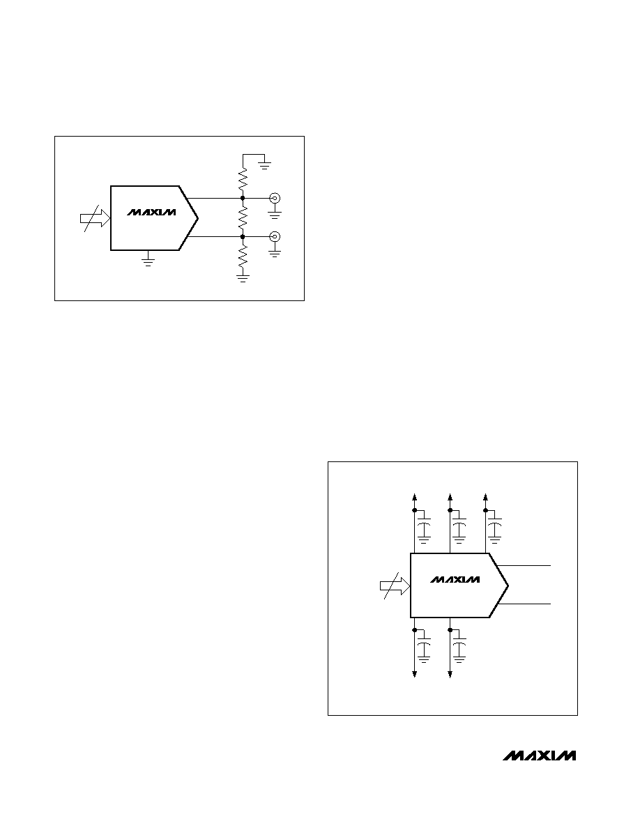
25
50
25
OUTP
OUTN
Figure 7. Differential Output Configuration
MAX5875
16
OUTIP/OUTQP
OUTIN/OUTQN
DATA15–DATA0
0.1
F
AVDD1.8
DVDD1.8
0.1
F
0.1
F
0.1
F
AVDD3.3
DVDD3.3
0.1
F
AVCLK
BYPASSING—DAC LEVEL
*BYPASS EACH POWER-SUPPLY PIN INDIVIDUALLY.
Figure 8. Recommended Power-Supply Decoupling and
Bypassing Circuitry
相关PDF资料 |
PDF描述 |
|---|---|
| MAX5876EGK+D | IC DAC 12BIT DUAL 250MSPS 68-QFN |
| MAX5877EGK+D | IC DAC 14BIT DUAL 250MSPS 68-QFN |
| MAX5878EGK+D | IC DAC 16BIT DUAL 250MSPS 68-QFN |
| MAX5884EGM+D | IC DAC 14BIT 3.3V 200MSPS 48-QFN |
| MAX5885EGM+D | IC DAC 16BIT 3.3V 200MSPS 48-QFN |
相关代理商/技术参数 |
参数描述 |
|---|---|
| MAX5875EGK-TD | 功能描述:数模转换器- DAC RoHS:否 制造商:Texas Instruments 转换器数量:1 DAC 输出端数量:1 转换速率:2 MSPs 分辨率:16 bit 接口类型:QSPI, SPI, Serial (3-Wire, Microwire) 稳定时间:1 us 最大工作温度:+ 85 C 安装风格:SMD/SMT 封装 / 箱体:SOIC-14 封装:Tube |
| MAX5875EVKIT | 功能描述:数模转换器- DAC Evaluation Kit for the MAX5873 MAX5874 MAX5875 RoHS:否 制造商:Texas Instruments 转换器数量:1 DAC 输出端数量:1 转换速率:2 MSPs 分辨率:16 bit 接口类型:QSPI, SPI, Serial (3-Wire, Microwire) 稳定时间:1 us 最大工作温度:+ 85 C 安装风格:SMD/SMT 封装 / 箱体:SOIC-14 封装:Tube |
| MAX5876EGK | 制造商:Rochester Electronics LLC 功能描述: 制造商:Maxim Integrated Products 功能描述: |
| MAX5876EGK+D | 功能描述:数模转换器- DAC 12-Bit 2Ch 250Msps DAC RoHS:否 制造商:Texas Instruments 转换器数量:1 DAC 输出端数量:1 转换速率:2 MSPs 分辨率:16 bit 接口类型:QSPI, SPI, Serial (3-Wire, Microwire) 稳定时间:1 us 最大工作温度:+ 85 C 安装风格:SMD/SMT 封装 / 箱体:SOIC-14 封装:Tube |
| MAX5876EGK+TD | 功能描述:数模转换器- DAC 12-Bit 2Ch 250Msps DAC RoHS:否 制造商:Texas Instruments 转换器数量:1 DAC 输出端数量:1 转换速率:2 MSPs 分辨率:16 bit 接口类型:QSPI, SPI, Serial (3-Wire, Microwire) 稳定时间:1 us 最大工作温度:+ 85 C 安装风格:SMD/SMT 封装 / 箱体:SOIC-14 封装:Tube |
发布紧急采购,3分钟左右您将得到回复。