- 您现在的位置:买卖IC网 > Datasheet目录43 > MAX5926EEE+ (Maxim Integrated)IC HOT-SWAP CONTROLLER 16QSOP-EP Datasheet资料下载
参数资料
| 型号: | MAX5926EEE+ |
| 厂商: | Maxim Integrated |
| 文件页数: | 2/21页 |
| 文件大小: | 333K |
| 描述: | IC HOT-SWAP CONTROLLER 16QSOP-EP |
| 产品培训模块: | Lead (SnPb) Finish for COTS Obsolescence Mitigation Program |
| 标准包装: | 100 |
| 类型: | 热交换控制器 |
| 应用: | 通用 |
| 内部开关: | 无 |
| 电源电压: | 1 V ~ 13.2 V |
| 工作温度: | -40°C ~ 85°C |
| 安装类型: | 表面贴装 |
| 封装/外壳: | 16-LSSOP(0.154",3.90mm 宽) |
| 供应商设备封装: | 16-QSOP 裸露焊盘 |
| 包装: | 管件 |
1V to 13.2V, n-Channel Hot-Swap Controllers
Require No Sense Resistor
2 _______________________________________________________________________________________
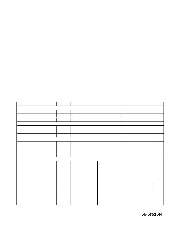
ABSOLUTE MAXIMUM RATINGS
ELECTRICAL CHARACTERISTICS
(V
CC
, EN (MAX5924/MAX5925), EN1 (MAX5926) = +2.7V to +13.2V; EN2 (MAX5926) = 0V; V
S
(see Figure 1) = +1.05V to V
CC
;
T
A
= -40癈 to +85癈, unless otherwise noted. Typical values are at V
CC
= 5V, R
L
= 500& from OUT to GND, C
L
= 1礔, SLEW =
open, T
A
= +25癈, unless otherwise noted.) (Note 1)
Stresses beyond those listed under
Absolute Maximum Ratings
may cause permanent damage to the device. These are stress ratings only, and functional
operation of the device at these or any other conditions beyond those indicated in the operational sections of the specifications is not implied. Exposure to
absolute maximum rating conditions for extended periods may affect device reliability.
(All voltages referenced to GND, unless otherwise noted.)
V
CC
.........................................................................-0.3V to +14V
GATE*.....................................................................-0.3V to +20V
All Other Pins ............-0.3V to the lower of (V
CC
+ 0.3V) or +14V
SC_DET Current (200ms pulse width, 15% duty cycle) ...140mA
Continuous Current (all other pins).....................................20mA
Continuous Power Dissipation (T
A
= +70癈)
10-Pin 礛AX (derate 6.9mW/癈 above +70癈)...........556mW
16-Pin QSOP (derate 18.9mW/癈 above +70癈).......1509mW
Operating Temperature Range ...........................-40癈 to +85癈
Junction Temperature .....................................................+150癈
Storage Temperature Range.............................-65癈 to +150癈
Lead Temperature (soldering, 10s).................................+300癈
Soldering Temperature (reflow).......................................+260癈
PARAMETER
SYMBOL
CONDITIONS
MIN
TYP
MAX
UNITS
POWER SUPPLIES
V
CC
Operating Range
V
CC
2.7
13.2
V
V
S
Operating Range
V
S
V
S
as defined in Figure 1
1.0
V
CC
V
Supply Current
I
CC
FET is fully enhanced, SC_DET = V
CC
1.5
2.5
mA
UNDERVOLTAGE LOCKOUT (UVLO)
UVLO Threshold
V
UVLO
D efaul
t val
ue, V
S
and V
C C
i ncr easi ng , Fi g ur e 1
1.73
2.06
2.47
V
V
CC
UVLO Deglitch Time
t
DG
(Note 2)
900
祍
V
CC
UVLO Startup Delay
t
D UVLO
123
200
350
ms
LOAD-PROBE
2.7V < V
CC
< 5V
4
30
65
Load-Probe Resistance (Note 3)
R
LP
5V < V
CC
< 13.2V
3
10
20
&
Load-Probe Timeout
t
LP
43
102
205
ms
Load-Probe Threshold Voltage
V
LP,TH
(Note 4)
172
200
235
mV
CIRCUIT BREAKER
V
CC
= 2.7V and V
CB
= 1V
37
I
CB
TC = high
(MAX5926), MAX5924
2.7V d V
CC
d 13.2V
34
37
42
V
CC
= 2.7V, V
CB
=
1V, T
A
= +25癈
30
40
50
I
CB25
TC = low (MAX5926),
MAX5925 (Note 5)
2.7V d V
CC
d 13.2V,
T
A
= +25癈
40
50
60
V
CC
= 2.7V and V
CB
= 1V, T
A
= +85癈
40
50
60
Circuit-Breaker Programming
Current
I
CB85
TC = low (MAX5926),
MAX5925 (Note 5)
2.7V d V
CC
d 13.2V,
T
A
= +85癈
50
60
70
礎
*GATE is internally driven and clamped. Do not drive GATE with external source.
相关PDF资料 |
PDF描述 |
|---|---|
| MAX5929BEEG+ | IC HOT SWAP CTLR QUAD 24QSOP |
| MAX5930AEEG+ | IC HOT SWAP CTLR PWR SEQ 24QSOP |
| MAX5932ESA+T | IC HOT-SWAP CONTROLLER 8-SOIC |
| MAX5933EESA+ | IC HOT-SWAP CONTROLLER 8-SOIC |
| MAX5934EEE+ | IC HOT-SWAP CONTROLLER 16-QSOP |
相关代理商/技术参数 |
参数描述 |
|---|---|
| MAX5926EEE+ | 功能描述:热插拔功率分布 1-13.2V Hot-Swap Controller RoHS:否 制造商:Texas Instruments 产品:Controllers & Switches 电流限制: 电源电压-最大:7 V 电源电压-最小:- 0.3 V 工作温度范围: 功率耗散: 安装风格:SMD/SMT 封装 / 箱体:MSOP-8 封装:Tube |
| MAX5926EEE+T | 功能描述:热插拔功率分布 1-13.2V Hot-Swap Controller RoHS:否 制造商:Texas Instruments 产品:Controllers & Switches 电流限制: 电源电压-最大:7 V 电源电压-最小:- 0.3 V 工作温度范围: 功率耗散: 安装风格:SMD/SMT 封装 / 箱体:MSOP-8 封装:Tube |
| MAX5926EEE-T | 功能描述:热插拔功率分布 RoHS:否 制造商:Texas Instruments 产品:Controllers & Switches 电流限制: 电源电压-最大:7 V 电源电压-最小:- 0.3 V 工作温度范围: 功率耗散: 安装风格:SMD/SMT 封装 / 箱体:MSOP-8 封装:Tube |
| MAX5926EVKIT | 制造商:Maxim Integrated Products 功能描述:1V TO 13.2V N-CHANNEL HOT-SWAP CON - Rail/Tube |
| MAX5927AETJ+ | 功能描述:热插拔功率分布 Quad Hot-Swap Controller RoHS:否 制造商:Texas Instruments 产品:Controllers & Switches 电流限制: 电源电压-最大:7 V 电源电压-最小:- 0.3 V 工作温度范围: 功率耗散: 安装风格:SMD/SMT 封装 / 箱体:MSOP-8 封装:Tube |
发布紧急采购,3分钟左右您将得到回复。