- 您现在的位置:买卖IC网 > PDF目录19782 > MAX5936ANESA+T (Maxim Integrated)IC HOT-SWAP CTRLR -48V 8-SOIC PDF资料下载
参数资料
| 型号: | MAX5936ANESA+T |
| 厂商: | Maxim Integrated |
| 文件页数: | 10/23页 |
| 文件大小: | 382K |
| 描述: | IC HOT-SWAP CTRLR -48V 8-SOIC |
| 产品培训模块: | Lead (SnPb) Finish for COTS Obsolescence Mitigation Program |
| 标准包装: | 2,500 |
| 类型: | 热交换控制器 |
| 应用: | 通用 |
| 内部开关: | 无 |
| 电源电压: | -10 V ~ -80 V |
| 工作温度: | -40°C ~ 85°C |
| 安装类型: | 表面贴装 |
| 封装/外壳: | 8-SOIC(0.154",3.90mm 宽) |
| 供应商设备封装: | 8-SOIC |
| 包装: | 带卷 (TR) |
-48V Hot-Swap Controllers with V
IN
Step Immunity and No R
SENSE
10 ______________________________________________________________________________________
The V
IN
step immunity provides a means for transition-
ing through a large step increase in V
IN
with minimal
backplane inrush current and without shutting down
the load. Without V
IN
step immunity (when the power
MOSFET is fully enhanced), a step increase in V
IN
will
result in a high inrush current and a large step in V
OUT
,
which can trip the circuit breaker. With V
IN
step immu-
nity, the STEP_MON input detects the step before a
short circuit is detected at V
OUT
and alters the
MAX5936/MAX5937 response to V
OUT
exceeding
V
SC
due to the step. The 1.25V voltage threshold at
STEP_MON and a 10礎 current source at STEP_MON
allow the user to set the sensitivity of the step detection
with an external resistor to V
EE
. A capacitor is placed
between GND and the STEP_MON input, which, in con-
junction with the resistor, sets the STEP_MON time con-
stant. When a step is detected by the STEP_MON input
to rise above its threshold (STEP
TH
), the overcurrent
fault management is blocked and remains blocked as
long as STEP
TH
is exceeded. When STEP
TH
is exceed-
ed, the MAX5936/MAX5937 take no action until V
OUT
rises above V
SC
or above V
CB
for the 1.2ms circuit-
breaker glitch rejection period. When either of these
conditions occurs, a step GATE cycle begins and the
GATE is immediately brought to V
EE
, which turns off the
power MOSFET to minimize the resulting inrush current
surge from the backplane and PGOOD remains assert-
ed. GATE is held at V
EE
for 350祍, and after about 1ms,
begins to ramp up thereby enhancing the power
MOSFET in a controlled manner as in the power-up
GATE cycle. This provides a controlled inrush current
to charge the load capacitance to the new supply volt-
age (see the GATE Cycles section in Appendix A).
As in the case of the power-up GATE cycle, if V
OUT
drops to less than 72% of the programmed V
CB
, inde-
pendent of the state of STEP_MON, the GATE voltage
is rapidly pulled to full enhancement. PGOOD remains
asserted throughout the step. Otherwise, if the
STEP_MON input has decayed below its threshold but
V
OUT
remains above 72% of the programmed V
CB
(when GATE reaches 90% of full enhancement),
(a step-to-fault management fault has occurred). GATE
is rapidly pulled to V
EE
, turning off the power MOSFET
and disconnecting the load, PGOOD (PGOOD) is
deasserted, and the MAX5936/MAX5937 enter the fault
management mode.
Fault Management
Fault management can be triggered by the following
conditions:
" V
OUT
exceeds 72% of V
CB
during GATE ramp at
90% of full enhancement,
" V
OUT
exceeds the V
CB
for longer than 1.2ms during
full enhancement,
" V
OUT
exceeds the V
SC
during full enhancement, and
" Load-probe test fails.
Once in the fault management mode, GATE will always
be pulled to V
EE
to turn off the external MOSFET and
PGOOD (PGOOD) will always be deasserted. The
MAX5936A_/MAX5937A_ have automatic retry following
a fault while the MAX5936L_/MAX5937L remain latched
in the fault condition.
Autoretry Fault Management
(MAX5936A_/MAX5937A_)
If the MAX5936A_/MAX5937A_entered fault management
due to circuit-breaker and short-circuit faults, the
autoretry timer starts immediately. The timer times out in
3.5s (typ) and at the end of the timeout, the sequencer
initiates a load-probe test. If this is successful, it starts a
normal power-up GATE cycle.
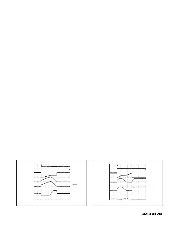
Figure 6. MAX5936 Response to a Step Input (V
OUT
< 0.74V
CB
)
V
IN
5V/div
V
PGOOD
20V/div
2ms/div
V
GATE
10V/div
V
OUT
20V/div
I
IN
1A/div
C
LOAD
= 100礔
R
LOAD
= 100&
40V
Figure 7. MAX5936 Response to a Step Input (V
OUT
> 0.74V
CB
)
V
IN
20V/div
V
PGOOD
50V/div
4ms/div
V
GATE
10V/div
V
OUT
50V/div
I
IN
5A/div
40V
20V
C
LOAD
= 100礔
R
LOAD
= 20&
相关PDF资料 |
PDF描述 |
|---|---|
| GQM1885C1H100JB01D | CAP CER 10PF 50V 5% NP0 0603 |
| VE-25Z-CX-F1 | CONVERTER MOD DC/DC 2V 30W |
| MAX5936ACESA+T | IC HOT-SWAP CTRLR -48V 8-SOIC |
| LCMXO1200E-3FT256I | IC PLD 1200LUTS 211I/O 256-BGA |
| MAX5937ABESA+T | IC HOT-SWAP CTRLR -48V 8-SOIC |
相关代理商/技术参数 |
参数描述 |
|---|---|
| MAX5936LAESA | 功能描述:热插拔功率分布 RoHS:否 制造商:Texas Instruments 产品:Controllers & Switches 电流限制: 电源电压-最大:7 V 电源电压-最小:- 0.3 V 工作温度范围: 功率耗散: 安装风格:SMD/SMT 封装 / 箱体:MSOP-8 封装:Tube |
| MAX5936LAESA+ | 功能描述:热插拔功率分布 48V- Hot-Swap Controller RoHS:否 制造商:Texas Instruments 产品:Controllers & Switches 电流限制: 电源电压-最大:7 V 电源电压-最小:- 0.3 V 工作温度范围: 功率耗散: 安装风格:SMD/SMT 封装 / 箱体:MSOP-8 封装:Tube |
| MAX5936LAESA+T | 功能描述:热插拔功率分布 48V- Hot-Swap Controller RoHS:否 制造商:Texas Instruments 产品:Controllers & Switches 电流限制: 电源电压-最大:7 V 电源电压-最小:- 0.3 V 工作温度范围: 功率耗散: 安装风格:SMD/SMT 封装 / 箱体:MSOP-8 封装:Tube |
| MAX5936LAESA-T | 功能描述:热插拔功率分布 RoHS:否 制造商:Texas Instruments 产品:Controllers & Switches 电流限制: 电源电压-最大:7 V 电源电压-最小:- 0.3 V 工作温度范围: 功率耗散: 安装风格:SMD/SMT 封装 / 箱体:MSOP-8 封装:Tube |
| MAX5936LBESA | 功能描述:热插拔功率分布 RoHS:否 制造商:Texas Instruments 产品:Controllers & Switches 电流限制: 电源电压-最大:7 V 电源电压-最小:- 0.3 V 工作温度范围: 功率耗散: 安装风格:SMD/SMT 封装 / 箱体:MSOP-8 封装:Tube |
发布紧急采购,3分钟左右您将得到回复。