- 您现在的位置:买卖IC网 > PDF目录19786 > MAX5937ANESA+T (Maxim Integrated)IC HOT-SWAP CTRLR -48V 8-SOIC PDF资料下载
参数资料
| 型号: | MAX5937ANESA+T |
| 厂商: | Maxim Integrated |
| 文件页数: | 20/23页 |
| 文件大小: | 382K |
| 描述: | IC HOT-SWAP CTRLR -48V 8-SOIC |
| 产品培训模块: | Lead (SnPb) Finish for COTS Obsolescence Mitigation Program |
| 标准包装: | 2,500 |
| 类型: | 热交换控制器 |
| 应用: | 通用 |
| 内部开关: | 无 |
| 电源电压: | -10 V ~ -80 V |
| 工作温度: | -40°C ~ 85°C |
| 安装类型: | 表面贴装 |
| 封装/外壳: | 8-SOIC(0.154",3.90mm 宽) |
| 供应商设备封装: | 8-SOIC |
| 包装: | 带卷 (TR) |
-48V Hot-Swap Controllers with V
IN
Step Immunity and No R
SENSE
20 ___________________________________________________
Verification of the Step
Monitor Timing
It is prudent to verify conclusively that all circuit-breaker
and short-circuit faults will be blocked for all ramp
rates. To do this, some form of graphical analysis is
recommended but first, find the value of ?/DIV>
L,eqv
of the
load by a series of ramp tests as indicated earlier.
These tests include evaluating the load with a series of
V
IN
ramps of increasing ramp rates and monitoring the
rate of V
OUT
rise during the ramp. Each V
IN
ramp
should have a constant slope. The V
OUT
response data
must be taken only during the positive ramp. Data
taken after V
IN
has leveled off at the new higher value
must not be used.
Figure 18 shows the load in parallel with the load
capacitor, C
LOAD
, and the parallel connection in series
with the power MOSFET, which is fully enhanced with
V
GS
= 10V. The objective is to determine ?/DIV>
L,eqv
from
the V
OUT
response.
Figure 19 shows the general response of V
OUT
to a V
IN
ramp over time t. Equation 1 gives the response of V
OUT
to a ramp of dV/dt. The product (dV/dt) x ?/DIV>
C
=
V
OUT
(max) or the maximum V
OUT
voltage differential if
the V
IN
ramp were to continue indefinitely. The parame-
ter of interest is V
OUT
due to the ramp dV/dt, thus it is
necessary to subtract the DC shift in V
OUT
due to the
load resistance. For some loads, which are relatively
independent of supply voltage, this may be insignificant.
V
OUT
(t) = V
OUT
(t) - R
DS(ON)
x I
LOAD
where I
LOAD
is a function of the V
OUT
level that should
be determined separately with DC tests.
At any time (t) the V
OUT
fraction of V
OUT
(max) is:
V
OUT
(t) / [(dV/dt) x ?/DIV>
C
] = (1-e
(-t / 腖,eqv)
)
If V
OUT
(t) is measured at time t, then the equivalent
time constant of the load is found from:
?/DIV>
L,eqv
= -t / ln(1 - V
OUT
/ [(dV/dt) x ?/DIV>
C
])
As mentioned earlier, several measurements of V
OUT
at times t1, t2, t3, and t4 should be made during the
ramp. Each of these may result in slightly different val-
ues of ?/DIV>
L,eqv
and all values should then be averaged.
In making the measurements, the V
IN
ramp duration
should be such that V
OUT
reaches 2 or 3 times the
selected V
SC
. The ramp tests should include three
ramp rates: V
SC
/ ?/DIV>
C
, 2 x V
SC
/ ?/DIV>
C
and 4 x V
SC
/ ?/DIV>
C
.
The values of ?/DIV>
L,eqv
may vary over the range of slew
rates due to measurement error, nonlinear dynamics in
the load, and due to the fact that Equation 1 is a simpli-
fication from a higher order dynamic system. The
resulting range of ?/DIV>
L,eqv
values should be used to vali-
date the performance of the final design.
Having ?/DIV>
C
, ?/DIV>
L,eqv
, R
STEP
, and C
STEP
in a graphical
analysis using Equation 1 and Equation 2 can verify the
step monitor function by displaying the relative timing
of t
CB
, t
STEP
, and t
SC
, which are the times when V
CB
,
V
STEP_MON
, and V
SC
voltage thresholds are exceeded.
A simple spreadsheet for this purpose can be supplied
by Maxim upon request. Figures 20, 21, and 22 graphi-
cally verify a particular solution over 3 decades of V
IN
ramp rates. In addition, Figure 22 verifies that this solu-
tion will block all circuit-breaker and short-circuit faults
for even the lowest V
IN
ramp that will cause V
OUT
to
exceed V
CB
.
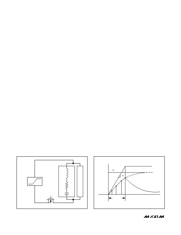
Figure 18. V
IN
Ramp Test of Load
L
EQU
R
EQV
C
LOAD
LOAD
LOAD CAPACITOR
WITH PARASITICS
V
IN
RAMP
10V
R
DS,ON
Figure 19. General Response of V
OUT
to a V
IN
Ramp
dv
dt
?/DIV>
C
dv
dt
V
IN
VOUT.F
VOUTi
V
IN
RAMP
0
t1 t2 t3 t4
相关PDF资料 |
PDF描述 |
|---|---|
| GMC44DRTI-S734 | CONN EDGECARD 88POS DIP .100 SLD |
| MAX5937LBESA+T | IC HOT-SWAP CTRLR -48V 8-SOIC |
| MAX5936ABESA+T | IC HOT-SWAP CTRLR -48V 8-SOIC |
| MAX5936AAESA+T | IC HOT-SWAP CTRLR -48V 8-SOIC |
| EBT156-6B1X | CONN EDGEBOARD SINGLE 6POS 5A |
相关代理商/技术参数 |
参数描述 |
|---|---|
| MAX5937LAESA | 功能描述:热插拔功率分布 RoHS:否 制造商:Texas Instruments 产品:Controllers & Switches 电流限制: 电源电压-最大:7 V 电源电压-最小:- 0.3 V 工作温度范围: 功率耗散: 安装风格:SMD/SMT 封装 / 箱体:MSOP-8 封装:Tube |
| MAX5937LAESA+ | 功能描述:热插拔功率分布 48V- Hot-Swap Controller RoHS:否 制造商:Texas Instruments 产品:Controllers & Switches 电流限制: 电源电压-最大:7 V 电源电压-最小:- 0.3 V 工作温度范围: 功率耗散: 安装风格:SMD/SMT 封装 / 箱体:MSOP-8 封装:Tube |
| MAX5937LAESA+T | 功能描述:热插拔功率分布 48V- Hot-Swap Controller RoHS:否 制造商:Texas Instruments 产品:Controllers & Switches 电流限制: 电源电压-最大:7 V 电源电压-最小:- 0.3 V 工作温度范围: 功率耗散: 安装风格:SMD/SMT 封装 / 箱体:MSOP-8 封装:Tube |
| MAX5937LAESA-T | 功能描述:热插拔功率分布 RoHS:否 制造商:Texas Instruments 产品:Controllers & Switches 电流限制: 电源电压-最大:7 V 电源电压-最小:- 0.3 V 工作温度范围: 功率耗散: 安装风格:SMD/SMT 封装 / 箱体:MSOP-8 封装:Tube |
| MAX5937LBESA | 功能描述:热插拔功率分布 RoHS:否 制造商:Texas Instruments 产品:Controllers & Switches 电流限制: 电源电压-最大:7 V 电源电压-最小:- 0.3 V 工作温度范围: 功率耗散: 安装风格:SMD/SMT 封装 / 箱体:MSOP-8 封装:Tube |
发布紧急采购,3分钟左右您将得到回复。