- 您现在的位置:买卖IC网 > Datasheet目录43 > MAX5954LETX+T (Maxim Integrated)IC PCI EXP/HOT-PLUG CTRLR 36TQFN Datasheet资料下载
参数资料
| 型号: | MAX5954LETX+T |
| 厂商: | Maxim Integrated |
| 文件页数: | 17/22页 |
| 文件大小: | 1027K |
| 描述: | IC PCI EXP/HOT-PLUG CTRLR 36TQFN |
| 产品培训模块: | Lead (SnPb) Finish for COTS Obsolescence Mitigation Program |
| 标准包装: | 2,500 |
| 类型: | 热交换控制器 |
| 应用: | 通用型,PCI Express? |
| 内部开关: | 无 |
| 电源电压: | 3.3V,12V |
| 工作温度: | -40°C ~ 85°C |
| 安装类型: | 表面贴装 |
| 封装/外壳: | 36-WFQFN 裸露焊盘 |
| 供应商设备封装: | 36-TQFN 裸露焊盘(6x6) |
| 包装: | 带卷 (TR) |
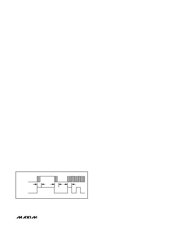
stays high for at least 4ms. After the debounce time,
OUTPUT follows INPUT. Figure 5 shows the timing dia-
gram describing the INPUT/OUTPUT debounced feature.
Present-Detect and Forced-On Inputs
(PPRREESS--D DEETT,, FFOONN)
PRES-DET input detects the PRSNT#2 pin on a PCI
Express connector. When the card is plugged in,
PRES-DET goes low and allows the turn-on of the out-
put after a 4ms debounced time. When the card is
removed, an internal 50k& pullup forces PRES-DET
high and the PCI Express slot is shut down with no
delay. PRES-DET works in conjunction with ON and
AUXON and only enables the device when ON and
AUXON are high.
A logic-low on FON forces the PCI Express slot (main
supplies and auxiliary) to turn on regardless of the sta-
tus of the other logic inputs provided the UVLO thresh-
olds are exceeded on all of the inputs.
Active Current Limits
Active current limits are provided for all three outputs.
Connect a current-sense resistor between 12S+ and
12S- to set the current limit for the 12V output. The cur-
rent limit is set to 54mV/R
SENSE12
. Connect a
current-sense resistor between 3.3S+ and 3.3S- to
set the current limit for the 3.3V main output to
20mV/R
SENSE3.3.
For the auxiliary output (3.3V
AUXO
)
the current limit is fixed at 470mA.
When the voltage across R
SENSE12
or R
SENSE3.3
reaches the current-limit threshold voltage, the
MAX5954 regulates the gate voltage to maintain the
current-limit threshold voltage across the sense resis-
tor. If the current limit lasts for t
FAULT
, then an overcur-
rent fault occurs. The MAX5954 shuts down both the
12V and 3.3V outputs and asserts the FAULT output.
When the auxiliary output reaches the current limit
(470mA) for longer than t
FAULT
, a fault occurs and the
device shuts down all outputs and asserts FAULT.
Undervoltage-Lockout Threshold
The UVLO thresholds prevent the internal auxiliary
MOSFET and the external main channel MOSFETs (Q1
and Q2 in the Typical Application Circuit) from turning
on if V
12VIN
, V
3.3VIN
, and V
3.3VAUXIN
are not present.
Internal comparators monitor the main supplies and the
auxiliary supply and keep the gate-drive outputs (12G
and 3.3G) low until the supplies rise above their UVLO
threshold. The 12V main supply is monitored at 12VIN
and has a UVLO threshold of 10V. The 3.3V main sup-
ply is monitored at 3.3S+ and has a UVLO threshold of
2.65V. The auxiliary supply is monitored at 3.3VAUXIN
and has a 2.65V UVLO threshold. For the main outputs to
operate, V
3.3VAUXIN
must be above its UVLO threshold.
External MOSFET Gate Driver
(12G and 3.3G)
The gate drive for the external MOSFETs is provided at
12G and 3.3G. 12G is the gate drive for the 12V main
supply and is boosted to 5.3V above V
12VIN
by an
internal charge pump. During turn-on, 12G sources
5礎 into the external gate capacitance to control the
turn-on time of the external MOSFET. During turn-off,
12G sinks 150礎 from the external gate capacitance to
quickly turn off the external MOSFET. During short-cir-
cuit events, an internal 120mA current activates to
rapidly bring the load current into the regulation limits.
3.3G is the gate drive for the 3.3V main supplys
MOSFET and is driven to 5.5V above the 3.3V main sup-
ply. The power for 3.3G is supplied from 12VIN and has
no internal charge pump. During turn-on, 3.3G sources
5礎 into the external gate capacitance to control the
turn-on time of the external MOSFET. During turn-off,
3.3G sinks 150礎 to quickly turn off the external
MOSFET. During short-circuit events, an internal 150mA
current activates to rapidly turn off the external
MOSFET.
Auxiliary Supply (3.3VAUXIN)
3.3VAUXIN provides power to the auxiliary output as
well as the internal logic and references. The drain of the
internal auxiliary MOSFET connects to 3.3VAUXIN
through internal sense resistor and the source connects
to the auxiliary output 3.3VAUXO. The MOSFETs typical
on-resistance is 0.3&. An internal charge pump boosts
the gate-drive voltage to fully turn on the internal n-chan-
nel MOSFET. The auxiliary supply has an internal current
limit set to 470mA.
Single PCI Express, Hot-Plug
Controller
______________________________________________________________________________________ 17
INPUT
DEBOUNCED
OUTPUT
t
DBC
t
DBC
t
DBC
Figure 5. INPUT and OUTPUT Debounced Feature
相关PDF资料 |
PDF描述 |
|---|---|
| MAX5955BEEE+ | IC DUAL HOT-SWAP CTRLR 16-QSOP |
| MAX5957AETN+T | IC TRPL PCI EXP/HOT-PLUG 56-TQFN |
| MAX5960AECS+T | IC CTRLR HOT-PLUG QD 80-TQFP |
| MAX5963UTL+T | IC HOT SWAP DIO ORING CTL 40TQFN |
| MAX5965AEAX+ | IC PSE CTRLR FOR POE 36SSOP |
相关代理商/技术参数 |
参数描述 |
|---|---|
| MAX5954LEVCMAXQUSB | 功能描述:电源管理IC开发工具 MAX5954LMAXQUSB EVAL KIT RoHS:否 制造商:Maxim Integrated 产品:Evaluation Kits 类型:Battery Management 工具用于评估:MAX17710GB 输入电压: 输出电压:1.8 V |
| MAX5954LEVKIT | 功能描述:电源管理IC开发工具 Evaluation Kit/Evaluation System for the MAX5954L/MAX5954A RoHS:否 制造商:Maxim Integrated 产品:Evaluation Kits 类型:Battery Management 工具用于评估:MAX17710GB 输入电压: 输出电压:1.8 V |
| MAX5955AEEE | 功能描述:热插拔功率分布 RoHS:否 制造商:Texas Instruments 产品:Controllers & Switches 电流限制: 电源电压-最大:7 V 电源电压-最小:- 0.3 V 工作温度范围: 功率耗散: 安装风格:SMD/SMT 封装 / 箱体:MSOP-8 封装:Tube |
| MAX5955AEEE+ | 功能描述:热插拔功率分布 Dual Hot-Swap Controller RoHS:否 制造商:Texas Instruments 产品:Controllers & Switches 电流限制: 电源电压-最大:7 V 电源电压-最小:- 0.3 V 工作温度范围: 功率耗散: 安装风格:SMD/SMT 封装 / 箱体:MSOP-8 封装:Tube |
| MAX5955AEEE+T | 功能描述:热插拔功率分布 Dual Hot-Swap Controller RoHS:否 制造商:Texas Instruments 产品:Controllers & Switches 电流限制: 电源电压-最大:7 V 电源电压-最小:- 0.3 V 工作温度范围: 功率耗散: 安装风格:SMD/SMT 封装 / 箱体:MSOP-8 封装:Tube |
发布紧急采购,3分钟左右您将得到回复。