- 您现在的位置:买卖IC网 > Datasheet目录43 > MAX5955BEEE+ (Maxim Integrated)IC DUAL HOT-SWAP CTRLR 16-QSOP Datasheet资料下载
参数资料
| 型号: | MAX5955BEEE+ |
| 厂商: | Maxim Integrated |
| 文件页数: | 2/15页 |
| 文件大小: | 354K |
| 描述: | IC DUAL HOT-SWAP CTRLR 16-QSOP |
| 产品培训模块: | Lead (SnPb) Finish for COTS Obsolescence Mitigation Program |
| 标准包装: | 100 |
| 类型: | 热交换控制器 |
| 应用: | 通用 |
| 内部开关: | 无 |
| 电源电压: | 1 V ~ 13.2 V |
| 工作温度: | -40°C ~ 85°C |
| 安装类型: | 表面贴装 |
| 封装/外壳: | 16-SSOP(0.154",3.90mm 宽) |
| 供应商设备封装: | 16-QSOP |
| 包装: | 管件 |
Low-Voltage, Dual Hot-Swap Controllers with
Independent On/Off Control
2 _______________________________________________________________________________________
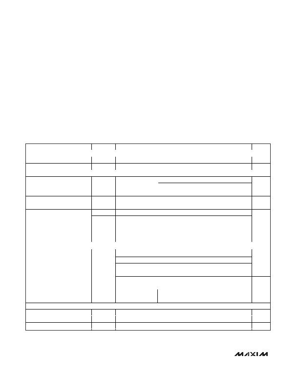
ABSOLUTE MAXIMUM RATINGS
ELECTRICAL CHARACTERISTICS
(V
IN_
= +1V to +13.2V provided at least one supply is higher than +2.7V, V
ON1
= V
ON2
= +2.7V, T
A
= T
MIN
to T
MAX
, unless otherwise
noted. Typical values are at V
IN1
= +5V, V
IN2
= +3.3V, and T
A
= +25癈.) (Note 1)
Stresses beyond those listed under
Absolute Maximum Ratings
may cause permanent damage to the device. These are stress ratings only, and functional
operation of the device at these or any other conditions beyond those indicated in the operational sections of the specifications is not implied. Exposure to
absolute maximum rating conditions for extended periods may affect device reliability.
IN_ to GND...........................................................................+14V
GATE_ to GND ...........................................-0.3V to (V
IN_
+ 6.2V)
ON_, PGOOD_, TIM to GND.......................-0.3V to the higher of
(V
IN1
+ 0.3V) and (V
IN2
+ 0.3V)
SENSE_, MON_, LIM_ to GND ...................-0.3V to (V
IN_
+ 0.3V)
Current into Any Pin .........................................................?0mA
Continuous Power Dissipation (T
A
= +70癈)
16-Pin QSOP (derate 8.3mW/癈 above +70癈)...........667mW
Operating Temperature Range
MAX59_ _ _U_ _...................................................0癈 to +85癈
MAX59_ _ _E_ _................................................-40癈 to +85癈
Storage Temperature Range.............................-65癈 to +150癈
Lead Temperature (soldering, 10s).................................+300癈
PARAMETER
SYMBOL
CONDITIONS
MIN
TYP
MAX
UNITS
POWER SUPPLIES
IN_ Input Voltage Range
V
IN
Other V
IN
e +2.7V
1.0
13.2
V
Supply Current
I
IN
I
IN1
+ I
IN2
, V
IN1
= +5V, V
IN2
= +3.3V
1.2
2.3
mA
CURRENT CONTROL
T
A
= +25癈
22.5
25
27.5
LIM = GND
T
A
= -40癈 to +85癈
20.5
27.5
Slow-Comparator Threshold
(V
IN
_ - V
SENSE
_) (Note 2)
V
SC,TH
R
LIM
= 300k&
80
100
130
mV
1mV overdrive
3
ms
Slow-Comparator Response Time
(Note 3)
t
SCD
10mV overdrive
110
祍
V
SU,TH
During startup
2 x V
SC
,
TH
Fast-Comparator Threshold
(V
IN
_ - V
SENSE
_)
V
FC,TH
V
IN
_ - V
SENSE
_; normal operation
4 x V
SC
,
TH
mV
Fast-Comparator Response Time
(V
IN
_ - V
SENSE
_)
t
FCD
10mV overdrive, from overload condition
260
ns
SENSE Input Bias Current
I
B SENSE
V
SENSE
_ = V
IN
_
0.03
1
礎
MOSFET DRIVER
R
TI M
=
100k&
6
10.8
16
R
TIM
= 4k& (minimum value)
0.31
0.45
0.58
Startup Period (Note 4)
t
START
TIM floating
4
9
17
ms
C har
g
i ng , V
GATE
_ =
+ 5V , V
IN
_ =
+ 10V ( N
ote 5)
65
100
130
礎
Average Gate Current
I
GATE
Discharging, triggered by a fault or when
V
ON_
< 0.875V
3
mA
V
IN
_ = 3V to 13.2V
4.8
5.4
6.0
Gate-Drive Voltage
V
DRIVE
V
GATE_
- V
IN
_,
I
GATE_
< 1礎
V
IN
_ = 2.7V to 3.0V
4.1
5.0
6.0
V
ON_ COMPARATOR
Low to high
0.85
0.875
0.90
V
ON_ Threshold
V
ON_
,
TH
Hysteresis
25
mV
ON_ Propagation Delay
10mV overdrive
50
祍
相关PDF资料 |
PDF描述 |
|---|---|
| MAX5957AETN+T | IC TRPL PCI EXP/HOT-PLUG 56-TQFN |
| MAX5960AECS+T | IC CTRLR HOT-PLUG QD 80-TQFP |
| MAX5963UTL+T | IC HOT SWAP DIO ORING CTL 40TQFN |
| MAX5965AEAX+ | IC PSE CTRLR FOR POE 36SSOP |
| MAX5969DETE+T | IC CTRLR INTERFCE W/MOSFT 16TQFN |
相关代理商/技术参数 |
参数描述 |
|---|---|
| MAX5955BEEE+ | 功能描述:热插拔功率分布 Dual Hot-Swap Controller RoHS:否 制造商:Texas Instruments 产品:Controllers & Switches 电流限制: 电源电压-最大:7 V 电源电压-最小:- 0.3 V 工作温度范围: 功率耗散: 安装风格:SMD/SMT 封装 / 箱体:MSOP-8 封装:Tube |
| MAX5955BEEE+T | 功能描述:热插拔功率分布 Dual Hot-Swap Controller RoHS:否 制造商:Texas Instruments 产品:Controllers & Switches 电流限制: 电源电压-最大:7 V 电源电压-最小:- 0.3 V 工作温度范围: 功率耗散: 安装风格:SMD/SMT 封装 / 箱体:MSOP-8 封装:Tube |
| MAX5955BEEE-T | 功能描述:热插拔功率分布 RoHS:否 制造商:Texas Instruments 产品:Controllers & Switches 电流限制: 电源电压-最大:7 V 电源电压-最小:- 0.3 V 工作温度范围: 功率耗散: 安装风格:SMD/SMT 封装 / 箱体:MSOP-8 封装:Tube |
| MAX5955BUEE | 功能描述:热插拔功率分布 RoHS:否 制造商:Texas Instruments 产品:Controllers & Switches 电流限制: 电源电压-最大:7 V 电源电压-最小:- 0.3 V 工作温度范围: 功率耗散: 安装风格:SMD/SMT 封装 / 箱体:MSOP-8 封装:Tube |
| MAX5955BUEE+ | 功能描述:热插拔功率分布 Dual Hot-Swap Controller RoHS:否 制造商:Texas Instruments 产品:Controllers & Switches 电流限制: 电源电压-最大:7 V 电源电压-最小:- 0.3 V 工作温度范围: 功率耗散: 安装风格:SMD/SMT 封装 / 箱体:MSOP-8 封装:Tube |
发布紧急采购,3分钟左右您将得到回复。