- 您现在的位置:买卖IC网 > PDF目录16884 > MAX6023EBT50+T (Maxim Integrated Products)IC VREF SERIES PREC 5V 5-UCSP PDF资料下载
参数资料
| 型号: | MAX6023EBT50+T |
| 厂商: | Maxim Integrated Products |
| 文件页数: | 12/13页 |
| 文件大小: | 0K |
| 描述: | IC VREF SERIES PREC 5V 5-UCSP |
| 产品培训模块: | Lead (SnPb) Finish for COTS Obsolescence Mitigation Program |
| 标准包装: | 2,500 |
| 基准类型: | 串联,精度 |
| 输出电压: | 5V |
| 容差: | ±0.2% |
| 温度系数: | 30ppm/°C |
| 输入电压: | 5.2 V ~ 12.6 V |
| 通道数: | 1 |
| 电流 - 静态: | 35µA |
| 电流 - 输出: | 500µA |
| 工作温度: | -40°C ~ 85°C |
| 安装类型: | 表面贴装 |
| 封装/外壳: | 5-WFBGA,CSPBGA |
| 供应商设备封装: | 5-UCSP(1.52x1.05) |
| 包装: | 带卷 (TR) |
�� �
�
�Precision,� Low-Power,� Low-Dropout,� UCSP�
�Voltage� Reference�
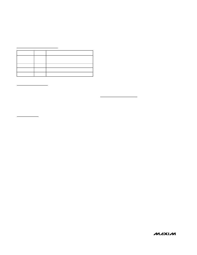
�Pin� Description�
�Output� Voltage� Hysteresis�
�Output� voltage� hysteresis� is� the� change� in� the� output�
�BUMP�
�A1,� A3�
�A2�
�B1�
�B3�
�NAME�
�I.C.�
�GND�
�OUT�
�IN�
�FUNCTION�
�Internally� connected.� Do� not�
�connect� to� this� pin.�
�Ground�
�Reference� Output�
�Input� Voltage�
�voltage� at� T� A� =� +25� °� C� before� and� after� the� device� is�
�cycled� over� its� entire� operating� temperature� range.�
�Hysteresis� is� caused� by� differential� package� stress�
�appearing� across� the� bandgap� core� transistors.� The�
�typical� temperature� hysteresis� value� is� 90ppm.�
�Turn-On� Time�
�These� devices� typically� turn� on� and� settle� within� 0.1%�
�of� their� final� value;� 30μs� to� 220μs� depending� on� the�
�Detailed� Description�
�The� MAX6023� precision� bandgap� references� use� a�
�proprietary� curvature� correction� circuit� and� laser-�
�trimmed� thin-film� resistor,� resulting� in� a� low� temperature�
�coefficient� of� <30ppm/� °� C� and� initial� accuracy� of� better�
�than� 0.2%.� These� devices� can� sink� and� source� up� to�
�500μA� with� <200mV� of� dropout� voltage,� making� them�
�attractive� for� use� in� low-voltage� applications.�
�Applications� Information�
�Output/Load� Capacitance�
�The� MAX6023� devices� do� not� require� an� output� capaci-�
�tor� for� dynamically� stable,� oscillation-free� operation.�
�They� are� stable� for� capacitive� loads� from� 0� to� 2.2nF.�
�However,� in� applications� where� the� load� or� the� supply�
�can� experience� step� changes,� an� output� capacitor�
�reduces� the� amount� of� overshoot� (or� undershoot)� and�
�improves� the� circuit� ’� s� transient� response.� Many� appli-�
�cations� do� not� need� an� external� capacitor� and� this� fam-�
�ily� offers� a� significant� advantage� in� these� applications�
�when� board� space� is� critical.�
�Supply� Current�
�The� no-load� supply� current� of� these� series-mode� refer-�
�ences� is� 35μA� maximum,� and� is� virtually� independent�
�of� the� supply� voltage,� with� only� a� 0.8μA/V� variation� from�
�the� supply� voltage.� Unlike� shunt-mode� references� that�
�must� draw� the� maximum� load� current� at� all� times,� the�
�load� current� is� drawn� from� the� input� voltage� source� only�
�when� required,� so� supply� current� is� not� wasted� and� effi-�
�ciency� is� maximized� at� all� input� voltages.� This� improved�
�efficiency� can� help� reduce� power� dissipation� and�
�extend� battery� life.�
�When� the� supply� voltage� is� below� the� minimum� speci-�
�fied� input� voltage� (as� during� turn-on),� the� devices� can�
�draw� up� to� 200μA� beyond� the� nominal� supply� current.�
�The� input� voltage� source� must� be� capable� of� providing�
�this� current� to� ensure� reliable� turn-on.�
�device.� The� turn-on� time� can� increase� up� to� 1.5ms� with�
�the� device� operating� at� the� minimum� dropout� voltage�
�and� the� maximum� load.�
�UCSP� Information�
�UCSP� Package� Consideration�
�For� general� UCSP� package� information� and� PC� layout�
�considerations,� refer� to� the� Maxim� Application� Note:�
�UCSP� —� A� Wafer-Level� Chip-Scale� Package.�
�UCSP� Reliability�
�The� UCSP� represents� a� unique� package� that� greatly�
�reduces� board� space� compared� to� other� packages.�
�The� chip-scale� package� represents� a� unique� packag-�
�ing� form� factor� that� may� not� perform� as� well� as� a� pack-�
�aged� product� through� traditional� mechanical� reliability�
�tests.� UCSP� reliability� is� integrally� linked� to� the� user� ’� s�
�assembly� methods,� circuit� board� material,� and� usage�
�environment.� The� user� should� closely� review� these�
�areas� when� considering� use� of� a� chip-scale� package.�
�Performance� through� operating-life� test� and� moisture�
�resistance� remains� uncompromised.� The� wafer-fabrica-�
�tion� process� primarily� determines� the� performance.�
�Mechanical� stress� performance� is� a� greater� considera-�
�tion� for� chip-scale� packages.� Chip-scale� packages� are�
�attached� through� direct� solder� contact� to� the� user� ’� s� PC�
�board,� foregoing� the� inherent� stress� relief� of� a� pack-�
�aged� product� lead� frame.� Solder� joint� contact� integrity�
�must� be� considered.� Comprehensive� reliability� tests�
�have� been� performed� and� are� available� upon� request.�
�In� conclusion,� the� UCSP� performs� reliably� through� envi-�
�ronmental� stresses.�
�12�
�______________________________________________________________________________________�
�相关PDF资料 |
PDF描述 |
|---|---|
| MAX6023EBT41+T | IC VREF SERIES PREC 4.096V 5UCSP |
| 8532R-46L | INDUCTOR 5600UH POWER SMD |
| MAX6191CESA+ | IC VREF SERIES PREC 2.048V 8SOIC |
| MAX6194CESA+ | IC VREF SERIES PREC 4.5V 8-SOIC |
| MAX6138BEXR33+T | IC VREF SHUNT PREC 3.3V SC-70-3 |
相关代理商/技术参数 |
参数描述 |
|---|---|
| MAX6025 | 制造商:MAXIM 制造商全称:Maxim Integrated Products 功能描述:+5V.Serial-Input.Voltage-Output 16-Bit DACs[MAX541/MAX542/MAX541/MAX542/MAX541/MAX542/MAX541ACPA/MAX541ACSA/MAX541ACSA-T/MAX541AEPA/MAX541AESA/MAX541AESA-T/MAX541BC/D/MAX541BCPA/MAX541BCSA/MAX541BCSA-T/MAX541BEPA/MAX541BESA/MAX541BESA-T/MAX541CCPA/MAX541C |
| MAX6025AEUR | 制造商:Maxim Integrated Products 功能描述:PRECISION LOW-POWER LOW-DROPOUT - Rail/Tube |
| MAX6025AEUR+ | 制造商:Maxim Integrated Products 功能描述:V-REF PRECISION 2.5V 0.5MA 3PIN SOT-23 - Rail/Tube 制造商:Maxim Integrated Products 功能描述:Voltage Reference,2.5V,MAX6025AEUR-T |
| MAX6025AEUR+T | 功能描述:基准电压& 基准电流 Low-Power Low-Drop Voltage Ref RoHS:否 制造商:STMicroelectronics 产品:Voltage References 拓扑结构:Shunt References 参考类型:Programmable 输出电压:1.24 V to 18 V 初始准确度:0.25 % 平均温度系数(典型值):100 PPM / C 串联 VREF - 输入电压(最大值): 串联 VREF - 输入电压(最小值): 分流电流(最大值):60 mA 最大工作温度:+ 125 C 封装 / 箱体:SOT-23-3L 封装:Reel |
| MAX6025AEUR+T | 制造商:Maxim Integrated Products 功能描述:IC LDO SERIES V-REF 2.5V 0.2% 3-SOT-23 制造商:Maxim Integrated Products 功能描述:IC, LDO SERIES V-REF, 2.5V 0.2% 3-SOT-23 |
发布紧急采购,3分钟左右您将得到回复。