- 您现在的位置:买卖IC网 > PDF目录1844 > MAX618EEE+T (Maxim Integrated Products)IC REG BOOST ADJ 0.5A 16QSOP PDF资料下载
参数资料
| 型号: | MAX618EEE+T |
| 厂商: | Maxim Integrated Products |
| 文件页数: | 6/14页 |
| 文件大小: | 0K |
| 描述: | IC REG BOOST ADJ 0.5A 16QSOP |
| 产品培训模块: | Lead (SnPb) Finish for COTS Obsolescence Mitigation Program |
| 标准包装: | 2,500 |
| 类型: | 升压(升压) |
| 输出类型: | 可调式 |
| 输出数: | 1 |
| 输出电压: | 可调至 28V |
| 输入电压: | 3 V ~ 28 V |
| PWM 型: | 混合物 |
| 频率 - 开关: | 250kHz |
| 电流 - 输出: | 500mA |
| 同步整流器: | 无 |
| 工作温度: | -40°C ~ 85°C |
| 安装类型: | 表面贴装 |
| 封装/外壳: | 16-SSOP(0.154",3.90mm 宽) |
| 包装: | 带卷 (TR) |
| 供应商设备封装: | 16-QSOP |
�� �
�
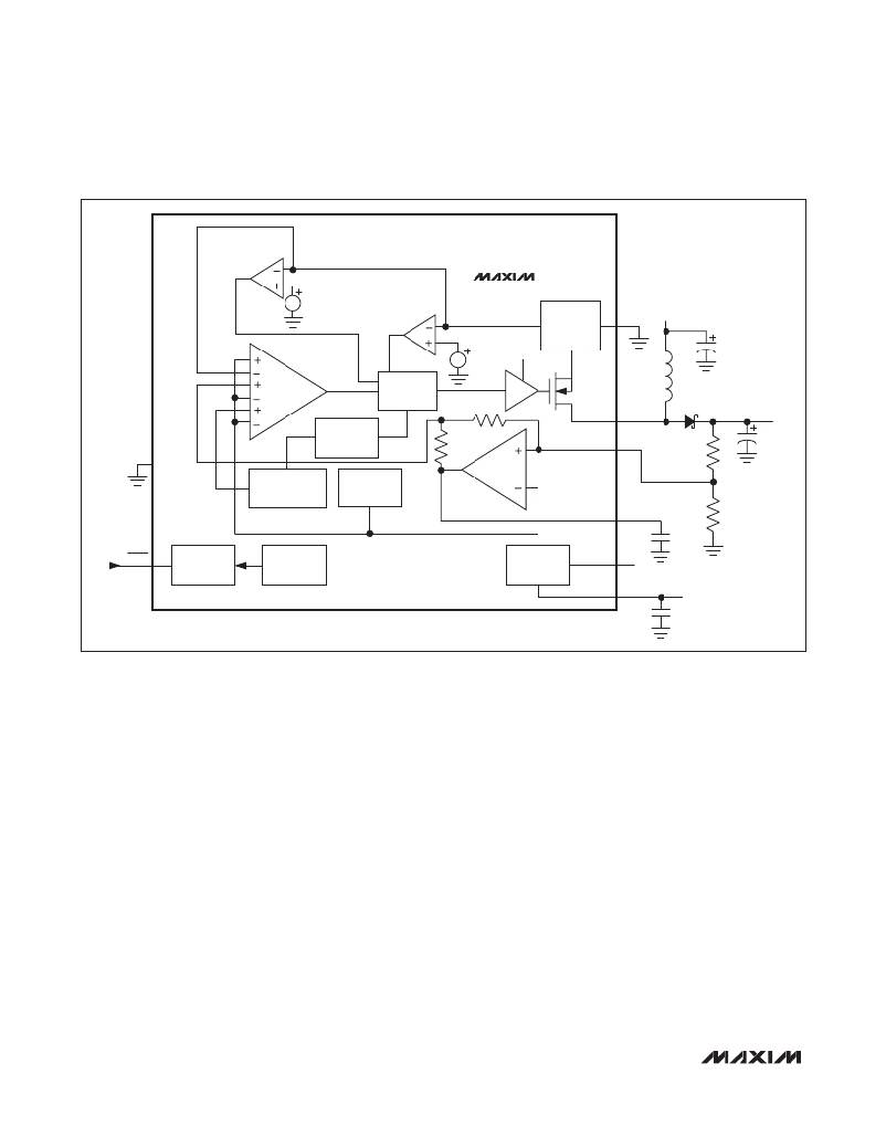
�28V,� PWM,� Step-Up� DC-DC� Converter�
�IDLE� MODE�
�CURRENT� LIMIT�
�MAX618�
�PWM�
�CURRENT� LIMIT�
�CURRENT-�
�SENSE�
�PGND�
�IN�
�CIRCUIT�
�VL�
�ERROR�
�COMPARATOR�
�PWM�
�LOGIC�
�NMOS�
�250kHz�
�R�
�LX�
�OUT�
�GND�
�SLOPE�
�COMPENSATION�
�OSCILLATOR�
�REFERENCE�
�14R�
�INTEGRATOR�
�FB�
�COMP�
�SHDN�
�SHUTDOWN�
�THERMAL�
�SHUTDOWN�
�LINEAR�
�REGULATOR�
�IN�
�VL�
�Figure� 2.� Functional� Diagram�
�the� output� capacitor.� Output� current� is� limited� by� the� 2A�
�MOSFET� current� limit� and� the� MAX618� ’s� package�
�power-dissipation� limit.� See� the� Maximum� Output�
�Current� section� for� details.�
�In� Idle� Mode,� the� MAX618� improves� light-load� efficien-�
�cy� by� reducing� inductor� current� and� skipping� cycles� to�
�reduce� the� losses� in� the� internal� switch,� diode,� and�
�inductor.� In� this� mode,� a� switching� cycle� initiates� only�
�when� the� error� comparator� senses� that� the� output� volt-�
�age� is� about� to� drop� out� of� regulation.� When� this�
�occurs,� the� NMOS� switch� turns� on� and� remains� on� until�
�the� inductor� current� exceeds� the� nominal� 350mA� Idle�
�Mode� current� limit.�
�Refer� to� Table� 1� for� an� estimate� of� load� currents� at� which�
�the� MAX618� transitions� between� PWM� and� Idle� Mode.�
�Compensation� Scheme�
�Although� the� higher� loop� gain� of� voltage-controlled�
�architectures� tends� to� provide� tighter� load� regulation,�
�current-controlled� architectures� are� generally� easier� to�
�compensate� over� wide� input� and� output� voltage�
�ranges.� The� MAX618� uses� both� control� schemes� in� par-�
�allel:� the� dominant,� low-frequency� components� of� the�
�error� signal� are� tightly� regulated� with� a� voltage-control�
�loop,� while� a� current-control� loop� improves� stability� at�
�higher� frequencies.� Compensation� is� achieved� through�
�the� selection� of� the� output� capacitor� (C� OUT� ),� the� inte-�
�grator� capacitor� (C� COMP� ),� and� the� pole� capacitor� (C� P� )�
�from� FB� to� GND.� C� P� cancels� the� zero� formed� by� C� OUT�
�and� its� ESR.� Refer� to� the� Capacitor� Selection� section� for�
�guidance� on� selecting� these� capacitors.�
�VL� Low-Dropout� Regulator�
�The� MAX618� contains� a� 3.1V� low-dropout� linear� regula-�
�tor� to� power� internal� circuitry.� The� regulator’s� input� is� IN�
�and� its� output� is� VL.� The� IN� to� VL� dropout� voltage� is�
�100mV,� so� that� when� IN� is� less� than� 3.2V,� VL� is� typically�
�100mV� below� IN.� The� MAX618� still� operates� when� the�
�LDO� is� in� dropout,� as� long� as� VL� remains� above� the�
�2.7V� undervoltage� lockout.� Bypass� VL� with� a� 4.7� μF�
�ceramic� capacitor� placed� as� close� to� the� VL� and� GND�
�pins� as� possible.�
�6�
�_______________________________________________________________________________________�
�相关PDF资料 |
PDF描述 |
|---|---|
| MAX6198AESA/V+T | IC VREF SERIES PREC 4.096V 8SOIC |
| MAX619ESA-T | IC REG SWITCHED CAP 5V 8SOIC |
| MAX6220ASA-4.1+T | IC VREF SERIES PREC 4.096V 8SOIC |
| MAX6250BCSA-T | IC VREF SERIES BURIED ZNR 8-SOIC |
| MAX629ESA-T | IC REG MULTI CONFIG +/-28V 8SOIC |
相关代理商/技术参数 |
参数描述 |
|---|---|
| MAX618EVKIT | 功能描述:直流/直流开关转换器 Evaluation Kit for the MAX618 RoHS:否 制造商:STMicroelectronics 最大输入电压:4.5 V 开关频率:1.5 MHz 输出电压:4.6 V 输出电流:250 mA 输出端数量:2 最大工作温度:+ 85 C 安装风格:SMD/SMT |
| MAX619 | 制造商:MAXIM 制造商全称:Maxim Integrated Products 功能描述:Regulated 5V Charge-Pump DC-DC Converter |
| MAX6190 | 制造商:MAXIM 制造商全称:Maxim Integrated Products 功能描述:Precision, Micropower, Low-Dropout Voltage References |
| MAX6190A | 制造商:MAXIM 制造商全称:Maxim Integrated Products 功能描述:Precision, Micropower, Low-Dropout Voltage References |
| MAX6190AESA | 功能描述:基准电压& 基准电流 Precision uPower Voltage Ref RoHS:否 制造商:STMicroelectronics 产品:Voltage References 拓扑结构:Shunt References 参考类型:Programmable 输出电压:1.24 V to 18 V 初始准确度:0.25 % 平均温度系数(典型值):100 PPM / C 串联 VREF - 输入电压(最大值): 串联 VREF - 输入电压(最小值): 分流电流(最大值):60 mA 最大工作温度:+ 125 C 封装 / 箱体:SOT-23-3L 封装:Reel |
发布紧急采购,3分钟左右您将得到回复。