- 您现在的位置:买卖IC网 > PDF目录1844 > MAX619ESA-T (Maxim Integrated Products)IC REG SWITCHED CAP 5V 8SOIC PDF资料下载
参数资料
| 型号: | MAX619ESA-T |
| 厂商: | Maxim Integrated Products |
| 文件页数: | 4/7页 |
| 文件大小: | 0K |
| 描述: | IC REG SWITCHED CAP 5V 8SOIC |
| 产品培训模块: | Lead (SnPb) Finish for COTS Obsolescence Mitigation Program |
| 标准包装: | 2,500 |
| 类型: | 切换式电容器(充电泵) |
| 输出类型: | 固定 |
| 输出数: | 1 |
| 输出电压: | 5V |
| 输入电压: | 2 V ~ 3.6 V |
| 频率 - 开关: | 500kHz |
| 电流 - 输出: | 50mA |
| 同步整流器: | 无 |
| 工作温度: | -40°C ~ 85°C |
| 安装类型: | 表面贴装 |
| 封装/外壳: | 8-SOIC(0.154",3.90mm 宽) |
| 包装: | 带卷 (TR) |
| 供应商设备封装: | 8-SOIC |
�� �
�
�Regulated� 5V� Charge-Pump�
�DC-DC� Converter�
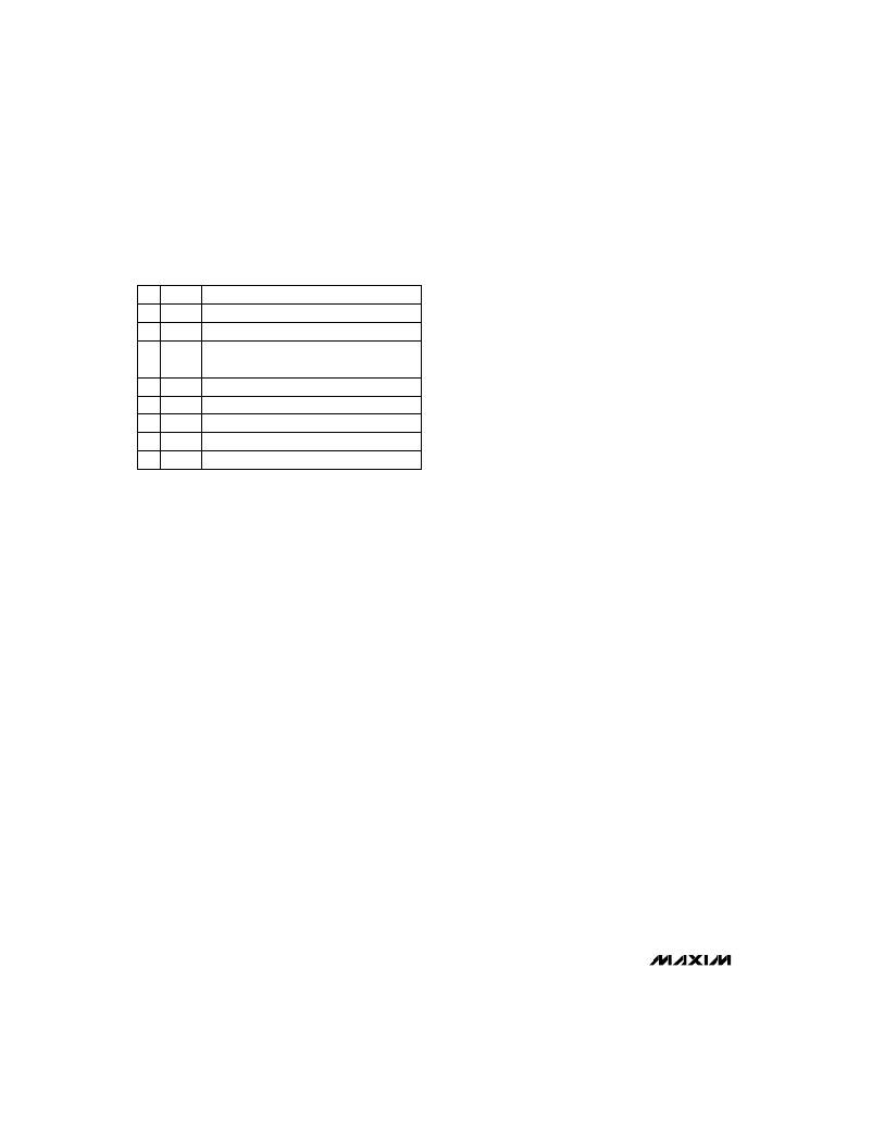
�_____________________Pin� Description�
�the� MAX619� switches� between� doubler� and� tripler�
�mode� on� alternating� cycles,� making� a� 2.5� x� V� IN� charge�
�PIN� NAME�
�1� C1+�
�FUNCTION�
�Positive� Terminal� for� C1�
�pump.� To� further� enhance� efficiency� over� the� input�
�range,� an� internal� comparator� selects� the� higher� of� V� IN�
�or� V� OUT� to� run� the� MAX619� ’s� internal� circuitry.�
�2�
�IN�
�Input� Supply� Voltage�
�Efficiency� with� V� IN� =� 2V� and� I� OUT� =� 20mA� is� typically�
�80%.�
�3�
�4�
�5�
�6�
�7�
�8�
�OUT�
�C2+�
�C2-�
�GND�
�SHDN�
�C1-�
�+5V� Output� Voltage.� V� OUT� =� 0V� when� in�
�shutdown� mode.�
�Positive� Terminal� for� C2�
�Negative� Terminal� for� C2�
�Ground�
�Active-High� CMOS� Logic-Level� Shutdown� Input�
�Negative� Terminal� for� C1�
�Figure� 1� shows� a� detailed� block� diagram� of� the�
�MAX619.� In� tripler� mode,� when� the� S1� switches� close,�
�the� S2� switches� open� and� capacitors� C1� and� C2�
�charge� up� to� V� IN� .� On� the� second� half� of� the� cycle,� C1�
�and� C2� are� connected� in� series� between� IN� and� OUT�
�when� the� S1� switches� open� and� the� S2� switches� close,�
�as� shown� in� Figure� 1.� In� doubler� mode,� only� C2� is�
�used.�
�During� one� oscillator� cycle,� energy� is� transferred� from�
�the� input� to� the� charge-pump� capacitors,� and� then�
�_______________Detailed� Description�
�Operating� Principle�
�The� MAX619� provides� a� regulated� 5V� output� from� a� 2V�
�to� 3.6V� (two� battery� cells)� input.� Internal� charge� pumps�
�and� external� capacitors� generate� the� 5V� output,� elimi-�
�nating� the� need� for� inductors.� The� output� voltage� is�
�regulated� to� 5V� ±4%� by� a� pulse-skipping� controller� that�
�turns� on� the� charge� pump� when� the� output� voltage�
�begins� to� droop.�
�To� maintain� the� greatest� efficiency� over� the� entire� input�
�voltage� range,� the� MAX619� ’s� internal� charge� pump�
�operates� as� a� voltage� doubler� when� V� IN� ranges� from�
�3.0V� to� 3.6V,� and� as� a� voltage� tripler� when� V� IN� ranges�
�from� 2.0V� to� 2.5V.� When� V� IN� ranges� from� 2.5V� to� 3.0V,�
�from� the� charge-pump� capacitors� to� the� output� capaci-�
�tor� and� load.� The� number� of� cycles� within� a� given� time�
�frame� increases� as� the� load� increases� or� as� the� input�
�supply� voltage� decreases.� In� the� limiting� case,� the�
�charge� pumps� operate� continuously,� and� the� oscillator�
�frequency� is� nominally� 500kHz.�
�Shutdown� Mode�
�The� MAX619� enters� low-power� shutdown� mode� when�
�SHDN� is� a� logic� high.� SHDN� is� a� CMOS-compatible�
�input.� In� shutdown� mode,� the� charge-pump� switching�
�action� is� halted,� OUT� is� disconnected� from� IN,� and�
�V� OUT� falls� to� 0V.� Connect� SHDN� to� ground� for� normal�
�operation.� When� V� IN� =� 3.6V,� V� OUT� typically� reaches�
�5V� in� 0.5ms� under� no-load� conditions� after� SHDN� goes�
�low.�
�4�
�________________________________________________________________________________________�
�相关PDF资料 |
PDF描述 |
|---|---|
| MAX6220ASA-4.1+T | IC VREF SERIES PREC 4.096V 8SOIC |
| MAX6250BCSA-T | IC VREF SERIES BURIED ZNR 8-SOIC |
| MAX629ESA-T | IC REG MULTI CONFIG +/-28V 8SOIC |
| MAX6304ESA | IC CIRCUIT SUPERVISORY LP 8-SOIC |
| MAX6306UK31D3-T | IC PROGRAM 3.080V RESET SOT23-5 |
相关代理商/技术参数 |
参数描述 |
|---|---|
| MAX619EVKIT | 制造商:MAXIM 制造商全称:Maxim Integrated Products 功能描述:Evaluation Kit for the MAX619 |
| MAX619EVKIT-SO | 功能描述:电荷泵 Evaluation Kit for the MAX619 RoHS:否 制造商:Maxim Integrated 功能:Inverting, Step Up 输出电压:- 1.5 V to - 5.5 V, 3 V to 11 V 输出电流:100 mA 电源电流:1 mA 最大工作温度:+ 70 C 封装 / 箱体:SOIC-8 Narrow 封装:Tube |
| MAX619MJA | 功能描述:电荷泵 RoHS:否 制造商:Maxim Integrated 功能:Inverting, Step Up 输出电压:- 1.5 V to - 5.5 V, 3 V to 11 V 输出电流:100 mA 电源电流:1 mA 最大工作温度:+ 70 C 封装 / 箱体:SOIC-8 Narrow 封装:Tube |
| MAX620 | 制造商:MAXIM 制造商全称:Maxim Integrated Products 功能描述:Quad, High-Side MOSFET Drivers |
| MAX620C/D | 功能描述:功率驱动器IC RoHS:否 制造商:Micrel 产品:MOSFET Gate Drivers 类型:Low Cost High or Low Side MOSFET Driver 上升时间: 下降时间: 电源电压-最大:30 V 电源电压-最小:2.75 V 电源电流: 最大功率耗散: 最大工作温度:+ 85 C 安装风格:SMD/SMT 封装 / 箱体:SOIC-8 封装:Tube |
发布紧急采购,3分钟左右您将得到回复。