- 您现在的位置:买卖IC网 > PDF目录132636 > MAX6471UT22BD2-T (MAXIM INTEGRATED PRODUCTS INC) RTC Module With CPU Supervisor PDF资料下载
参数资料
| 型号: | MAX6471UT22BD2-T |
| 厂商: | MAXIM INTEGRATED PRODUCTS INC |
| 元件分类: | 固定/可调正电压单路输出LDO稳压器 |
| 英文描述: | RTC Module With CPU Supervisor |
| 中文描述: | FIXED/ADJUSTABLE POSITIVE LDO REGULATOR, PDSO6 |
| 封装: | SOT-23, 6 PIN |
| 文件页数: | 12/20页 |
| 文件大小: | 896K |
| 代理商: | MAX6471UT22BD2-T |
MAX6469–MAX6484
300mA LDO Linear Regulators with Internal
Microprocessor Reset Circuit
2
_______________________________________________________________________________________
ABSOLUTE MAXIMUM RATINGS
(All voltages referenced to GND, unless otherwise noted.)
IN, SHDN, OUT, FB ..................................................-0.3V to +7V
MR, SET .......................................................-0.3V to (VIN + 0.3V)
RESET (push-pull) ...................................-0.3V to (VOUT + 0.3V)
RESET (open drain)..................................................-0.3V to +7V
OUT Short Circuit .......................................................Continuous
Input/Output Current (all pins except IN and OUT) ............20mA
Continuous Power Dissipation (TA = +70°C)
3 x 3 UCSP (derate 10.5mW/°C above +70°C) ............840mW
6-Pin SOT23 (derate 9.1mW/°C above +70°C).............727mW
8-Pin TDFN
(derate 24.4mW/°C above +70°C) ..............................1951mW
Operating Temperature Range ..........................-40°C to +85°C
Junction Temperature ......................................................+150°C
Storage Temperature Range .............................-65°C to +150°C
Lead Temperature (soldering, 10s) .................................+300°C
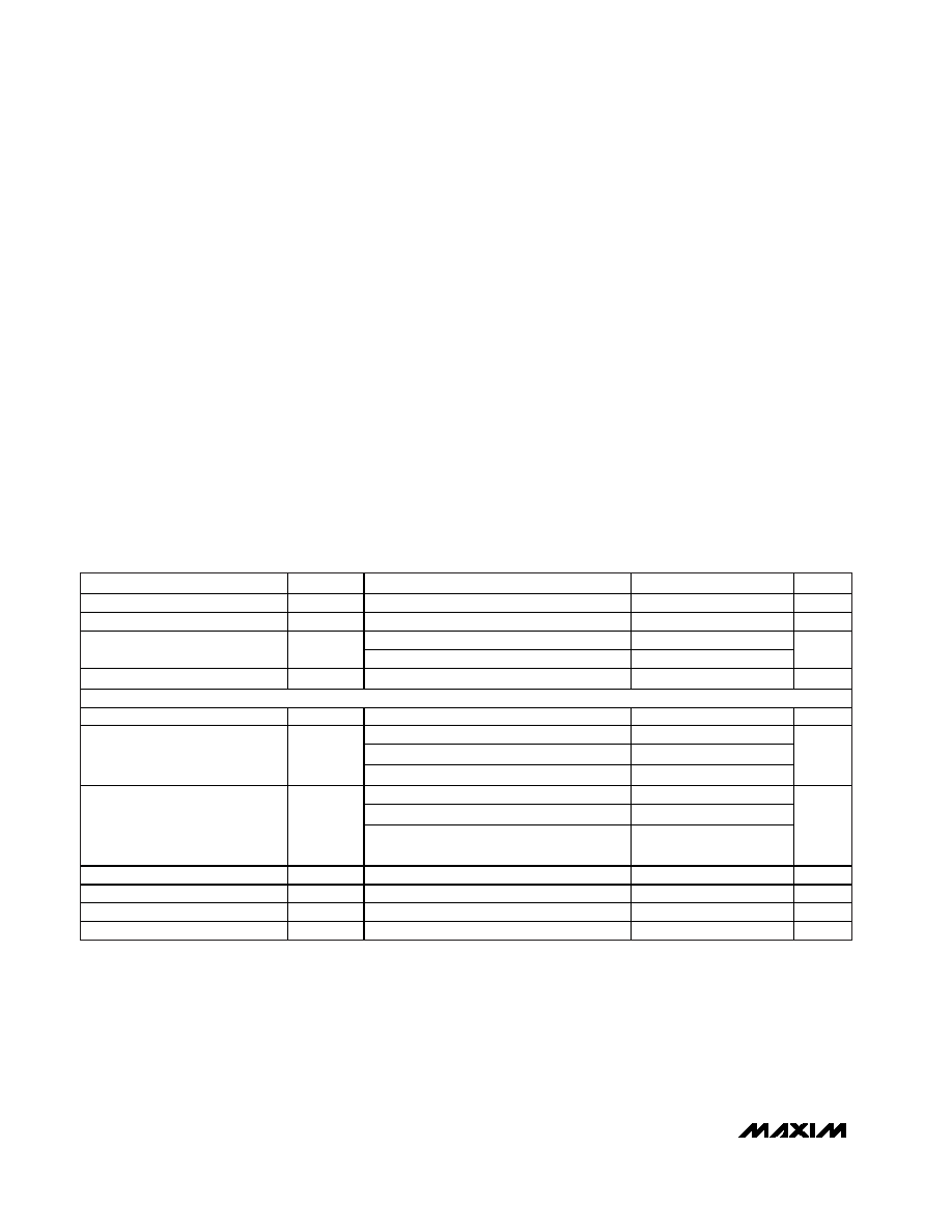
ELECTRICAL CHARACTERISTICS
(VIN = (VOUT + 0.5V) or +2.5V, whichever is greater, COUT = 3.3F, TA = -40°C to +85°C. Typical specifications are at TA = +25°C,
unless otherwise noted.) (Note 2)
PARAMETER
SYMBOL
CONDITIONS
MIN
TYP
MAX
UNITS
Input Voltage Range
VIN
2.5
5.5
V
Input Undervoltage Lockout
VUVLO
VIN falling
2.25
2.47
V
IOUT = 0
82
136
Supply Current (Ground Current)
IQ
IOUT = 300mA
96
A
Shutdown Supply Current
ISHDN
TA = +25°C
0.1
1
A
REGULATOR CIRCUIT
Output Current
300
mA
1mA
≤ IOUT ≤ 150mA, TA = +25°C
-1.3
+1.3
1mA
≤ IOUT ≤ 150mA, TA = -40°C to +85°C
-2.3
+2.3
Output Voltage Accuracy (Fixed
Output Voltage Operation,
Table 1) MAX6469–MAX6476
1mA
≤ IOUT ≤ 300mA, TA = -40°C to +85°C
-2.7
+2.7
%
2mA
≤ IOUT ≤ 100mA, TA = +25°C
-1.1
+1.1
2mA
≤ IOUT ≤ 100mA, TA = -40°C to +85°C
-2.0
+2.0
Output Voltage Accuracy (Fixed
Output Voltage Operation,
Table 1) MAX6477–MAX6484
2mA
≤ IOUT ≤ 300mA, TA = -40°C to +85°C
(Note 3)
-2.5
+2.5
%
Adjustable Output Voltage Range
VSET
5.0
V
SET Reference Voltage
VSET
1.200
1.229
1.258
V
SET Dual Mode
TM Threshold
185
mV
SET Input Leakage Current
ISET
VSET = 0, +1.2V (Note 3)
±20
±100
nA
Dual Mode is a trademark of Maxim Integrated Products, Inc.
Stresses beyond those listed under “Absolute Maximum Ratings” may cause permanent damage to the device. These are stress ratings only, and functional
operation of the device at these or any other conditions beyond those indicated in the operational sections of the specifications is not implied. Exposure to
absolute maximum rating conditions for extended periods may affect device reliability.
Note 1: The MAX6477–MAX6484 are constructed using a unique set of packaging techniques that impose a limit on the thermal pro-
file the devices can be exposed to during board-level solder attach and rework. This limit permits only the use of the solder
profiles recommended in the industry-standard specification, JEDEC 020A, paragraph 7.6, Table 3 for IR/VPR and
Convection reflow. Pre-heating is required. Hand or wave soldering is not allowed.
相关PDF资料 |
PDF描述 |
|---|---|
| MAX6471UT22BD3-T | RTC Module With CPU Supervisor |
| MAX6471UT22BD4-T | RTC Module With CPU Supervisor |
| MAX6471UT23AD1-T | RTC Module With CPU Supervisor |
| MAX6471UT23AD2-T | RTC Module With CPU Supervisor |
| MAX6471UT23AD3-T | RTC Module With CPU Supervisor |
相关代理商/技术参数 |
参数描述 |
|---|---|
| MAX6471UT22BD3 | 制造商:Maxim Integrated Products 功能描述:300MA LDO LINEAR REGULATORS WITH IN - Rail/Tube |
| MAX6471UT22BD3-T | 功能描述:低压差稳压器 - LDO RoHS:否 制造商:Texas Instruments 最大输入电压:36 V 输出电压:1.4 V to 20.5 V 回动电压(最大值):307 mV 输出电流:1 A 负载调节:0.3 % 输出端数量: 输出类型:Fixed 最大工作温度:+ 125 C 安装风格:SMD/SMT 封装 / 箱体:VQFN-20 |
| MAX6471UT22BD4 | 制造商:Maxim Integrated Products 功能描述:300MA LDO LINEAR REGULATORS WITH IN - Rail/Tube |
| MAX6471UT22BD4-T | 功能描述:低压差稳压器 - LDO RoHS:否 制造商:Texas Instruments 最大输入电压:36 V 输出电压:1.4 V to 20.5 V 回动电压(最大值):307 mV 输出电流:1 A 负载调节:0.3 % 输出端数量: 输出类型:Fixed 最大工作温度:+ 125 C 安装风格:SMD/SMT 封装 / 箱体:VQFN-20 |
| MAX6471UT23AD1 | 制造商:Maxim Integrated Products 功能描述:300MA LDO LINEAR REGULATORS WITH IN - Rail/Tube |
发布紧急采购,3分钟左右您将得到回复。